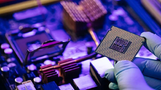
Printed circuit boards are the most important and basic component of the electronic industry. These boards have made it possible to create and run circuits on every level and have served as the backbone of any electronic device. With the growing demand for technology, PCBs have gone through multiple evolutions. The transformation of PCBs has made it possible to create innovative and better electronic circuits.
Today, we are talking about the emerging trends in PCB that are reshaping electronic circuits and the components used in innovative designs. But before this, it is important to understand the importance of using the emerging trends for the circuits.
Importance of Using Trending Technologies in PCBs
PCBs are versatile components, and not all PCBs are ideal for a particular type ...
Hello everyone and welcome to this article. Previously we have been discussing different types of PCB boards and for sure we have not exhausted everything. Today we are going to focus on a very important aspect of the PCB design which is the thermal characteristics of the PCB's working environment. Up to this moment, we have interacted with boards that work best in normal working conditions. But remember there are some working conditions, that have very harsh environment such as high temperatures. Let us take for example temperature in boilers or even electric heaters. Do you think normal FR-4 boards can survive in such temperatures? Don’t you think they will melt off if exposed to high thermal radiation? Your guess is as good as mine. For us to h ...
Hi readers! I hope you are having a great day and finding something new to learn. Today, the topic of our discourse is PCB Castellation and Castellated Holes.
Printed Circuit Boards (PCBs) are the core of nearly all electronic devices and are a structured platform on which components are mounted and interconnected. As electronics are moving toward more miniaturization, modularization, and mass production, PCB technologies must advance to be able to support these new requirements. Part of this advancement is the use of PCB castellations or castellated holes, a technology that supports small, modular board-to-board connections.
Castellated holes are tiny, plated half-holes on the border of a PCB. They allow one PCB, a module, or daughterboard, to be soldered onto another directly, much lik ...
Hello friends, I hope you all are doing great. Today, I am going to share the 10th chapter in the PCB learning series. So far, we have studied the basics of PCB i.e. What is PCB? Main Types of PCB, techniques to mount components on PCB etc. Now, we are ready to have a look at the complete PCB Fabrication Process.
So, in today's tutorial, I am going to share a detailed guide on PCB Fabrication Process. We will discuss everything related to it i.e. How PCB boards are manufactured? Which material is used to fabricate printed circuit boards? etc. But before starting the Fabrication PRocess, we first have to understand a few terms/features. So, let's get started:
PCB of DVD player:
RoHS-compliant P ...
Hello everyone and welcome to this article which will be a great introduction to high-speed PCB design. For sure it is going to be a very interesting class. Let me start by posing a question; Is this something that you have ever come across in your world of PCB design? Where you spent too much time doing the schematics, selecting the right components, doing the footprint addition, generating the netlists, doing the proper layout and routing and sending the end product of your design to the manufacturer? At this level you might probably be designing standard types of PCB boards and if someone was to introduce a project that talks about signal integrity, reflections or even crosstalk, very much believe you will feel like a lost person. It might be s ...
Hi readers! Welcome to this in-depth look at high-frequency PCB design. When dealing with radio frequency, microwave, or high-speed digital signals, you understand that the choice of material can ruin or redeem your design. FR-4 may be wonderful for typical-purpose PCBs, but it tends to lack in sophisticated applications. That is where Rogers PCB materials step in.
Rogers materials are laminates of high-performance that Rogers Corporation has made specifically for employment in RF and microwave circuit design applications. Their substrates contain low dielectric loss, reliable dielectric constants, and less moisture absorption. These characteristics are important for signal integrity, in particular, in high-frequency situations when even small changes can result in decreased performance.
...
Hello everyone. Today is a great day that we are going to put our focus on another type of PCB. So far in the previous articles, we have looked at high speed, metalcore, high density interconnect and the ceramic types of PCBs. In this article, we are going to introduce another type of PCB that might find great use in your day-to-day interaction with the printed circuit boards. it is very important for a designer to take note of how PCBs have evolved and how they have become an important aspect in the design of successful electronic devices. It has become hardly difficult to come across any time of an electronic device that does not involve the use of printed circuit boards.
In PCB boards you come across LEDs fixed in them, and due to the evolving w ...
Hey there, I hope you are having a good day. Printed circuit boards (PCBs) are a popular topic in the electronic world and we also know that PCBs have revolutionized circuits. They not only provide a solid base but the material used in the PCBs helps the circuit to function properly by protecting the circuit from factors like external radiation. These are present in different materials that divide the working, stability, and reliability of the circuit. In recent years, there has been a significant change in the types and strength of PCBs and this depends on the materials used in the manufacturing of these boards. We are interested in studying the advanced materials used in the manufacturing of PCBs and knowing the right type of material for the right circuit.
...
Hello friends, I hope everything's going well. Today, I am going to share the 13th chapter in the PCB learning series, where we will discuss the single-layer PCB in detail i.e. definition, construction, advantages, manufacturing, applications etc. So let’s try to absorb everything about the single-layer PCB:
Single-layer PCB overview:
Just a quick recall, PCB stands for a printed circuit board having different electrical components connected with the help of pads and tracks of copper foil, incorporated on an insulating material(substrate).
Single-layer PCBs have only one conductive layer of copper. The PCB board itself has a total of 3 layers in single-layer PCB other than the copper layer which are substrate, solder mask, and silkscreen.
In the past, phenolic aldehyde was us ...
Greetings and welcome to today’s lecture. It's our 7th tutorial in the PCB learning series. In our previous lectures, we have studied the two main types of PCB i.e. Single-sided and Double-sided PCB. Today is going to be a very interesting and interactive class about Through Hole Technology(THT), which is applied in the process of designing printed circuit boards.A PCB board has a properly designed circuit on it and it's composed of connecting traces/paths and various electronic components. The electronic components are mounted on the board in two different ways i.e. Through-hole and Surface-mount. We will cover Surface-mount in our next lecture and today, we will discuss how to mount components on PCB boards using though-hole technology.So, let's ...