Hi Friends! Hope you’re well today. I welcome you on board. Happy to see you around. In this post today, I’ll detail PCB Design Online Services for Engineering Students.
PCB designing is a crucial part of making some electrical projects. If you’re a student, you can leverage these services to design PCB online. You can design many PCB layouts for a single layer or multilayer PCB. Moreover, you can test simulation online and see how your design is working that you’re going to execute in real-time.
PCB Design Online Services for Engineering Students
You’ll find a list of online PCB design services. And I can understand, when you’re given a lot of options, it is very difficult to choose the best pick. The reason I have got you covered. In this post, ...
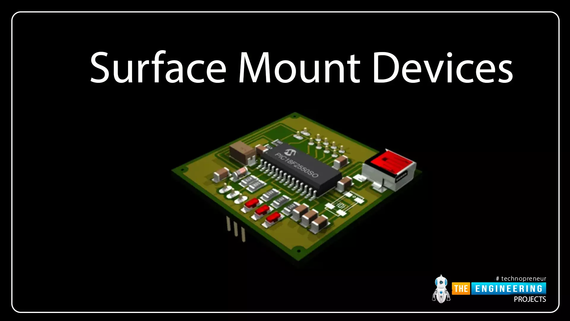
Greetings and welcome to today’s lecture. Today, we are going to focus our discussion on the Surface Mount Technology of PCB components mounting. It's our 8th tutorial in the PCB learning series and is going to be a very interesting and interactive class. In Surface-mount technology, SMT components(having small pads) are
placed on the surface of the PCB board and their pads are soldered on
the same side of the board.
As we discussed in our last lecture on Though-Hole Technology, there are two main methods used to mount components on PCB boards. We studied THT in the last lecture and today, we will focus on
Surface Mount Technology (SMT), we will discuss SMT classifications, types, applications, advantages and disadvantages in detail.
...
Hi Guys! Hope you’re well today. I welcome you on board. In this post, I’ll walk you through How to Optimize a PCB Panel Layout.
PCB panels are used in the manufacturing process to produce PCBs in large numbers. This not only reduces the overall cost but also makes the manufacturing process more efficient and reliable. PCB panelization is a manufacturing technique where multiple PCB designs are replicated on a single large board called a PCB panel. Then these individual boards are removed and depanelized from the panel to install them in the final product.
The number of panels is directly related to the overall manufacturing cost. To produce more panels, more cost will be required. However, it also depends on the shape of the board. If ...
Heat sinks are the electric routes for heat elimination from the PCB body. The digital electronic world is all about making devices compact and more powerful. This is possible only when the printed circuit boards (PCBs) are small enough to fit into the compact device. The increasing demand for power in low space comes with different challenges, of which the most crucial is the heat management of PCBs. The heat sinks are made of elements such as copper, aluminum, diamond, ceramic materials, graphite, etc., and play a crucial role in the thermal optimization of PCBs for optimal performance and long life. This comprehensive guide is about the basic introduction, heat transfer methods, key parameters, design considerations, and manufacturing techniques involved in the heat sink from the PCB po ...
The printed circuit board (PCB) is the backbone of electronic circuits, and for complex circuits, multi-layer PCBs are utilized to enhance productivity. PCB drilling is a crucial process, especially in multilayer PCB production, and involves precise via creation through laminate material. We know that vias are important conduits that bridge the gaps between multiple layers of PCBs. These are considered the conductive connections in a PCB, especially if it has multiple layers. Without vias, the multilayer PCBs have limited design flexibility and are impractical. In PCB manufacturing, there are multiple drilling types, but today I am going to discuss the comparison between the two most important methods, i.e. mechanical drilling and laser drilling.The appropriate drilling technique selection ...
Hello learners! Welcome to the introduction of the round PCBs, where we are going to discuss the round PCBs in detail. This is specially designed for articles for beginners as well as for intermediate skills in printed circuit boards. PCBs are the backbone of any circuit, and it is crucial to understand the type and application of the circuit and its PCB in detail before starting to work on it.
If you are going to buy crucial products like PCBs, always choose the best option that has positive reviews and a great experience. The best option for this is PCBWay.com, which has a great variety of PCBs, electronic components, equipment, and services. They have a vast variety of PCB services that range from high-speed PCBs to optical module PCBs, semiconductor tests, aerospace PCB circuit boa ...
Hello friends, I hope you all are doing great. Today, I am going to share the 10th chapter in the PCB learning series. So far, we have studied the basics of PCB i.e. What is PCB? Main Types of PCB, techniques to mount components on PCB etc. Now, we are ready to have a look at the complete PCB Fabrication Process.
So, in today's tutorial, I am going to share a detailed guide on PCB Fabrication Process. We will discuss everything related to it i.e. How PCB boards are manufactured? Which material is used to fabricate printed circuit boards? etc. But before starting the Fabrication PRocess, we first have to understand a few terms/features. So, let's get started:
PCB of DVD player:
RoHS-compliant P ...
Hi Fellas! I hope you all are having fun. Today, we will have a detailed overview of Flexible PCB. We will also understand why we need to use Flex PCB? What are its advantages & disadvantage? What kind of material is used? and How to manufacture flexible PCB? etc. Flexible PCB is the most advanced type of PCB, thus quite expensive and is normally used in industrial electronic products.
I'll try to explain everything related to flexible PCB so that you could get a clear idea of what is this about and what makes it stand out from other PCB boards? Let's dive in and explore the properties of flexible PCB one by one:
What is Flexible PCB?
Initially, PCBs were designed using hard substrate materials and th ...
Hey readers! Welcome to the penetrative guide to PCB manufacturing. Hopefully, you are doing well and looking for something great. The solder mask is the most vital component in manufacturing a printed circuit board (PCB), which guarantees reliability and ensures that everything functions smoothly.
These printed circuit boards serve as the backbone for almost all modern electronics, right from the simple household consumer products like a smartphone and a laptop to diverse applications such as industrial machinery and space equipment. A PCB provides physical and electrical connections and support for the components of electronics. The most crucial area for protection is the solder mask because of its great contribution to the copper behavior of an entire circuit regarding oxidation, dirt, ...
JLCPCB (JiaLiChuang Co. Limited) is a worldwide PCB & PCBA Fabrication enterprise. It is a leading company in high-tech manufacturing products specializing in PCB and PCBA production. With over a decade of experience in PCB manufacturing JLCPCB has made over a million customers through online ordering by the customers of PCB manufacturing and PCBA production.
JLCPCB is a professional manufacturer of large-scale manufacturing of PCBs, well equipment, strict management, and superior quality. It deals with the production of all types of PCBs, Stencils, and SMT.
In this article, we are going to discuss widely how the company operates its ordering system of the PCBs by their customers for production through the online booking process.
JLCPCB SMT ...