I remember the first time I handed off a PCB project without thinking hard enough about the assembly process. The board came back looking fine. Then we started testing. Footprint mismatch on a critical power IC. Wrong polarity on an electrolytic cap. Two components missing entirely. Three weeks of schedule gone. The factory had done exactly what we asked them to do. The problem was what we asked for.That experience taught me something most engineering programs never cover. The assembly model you choose matters as much as the circuit design itself. And turnkey PCB assembly is one of those decisions that gets made too casually, too often.What Turnkey PCB Assembly Actually Means
The word turnkey gets used loosely in manufacturing. In PCB assembly it ha ...
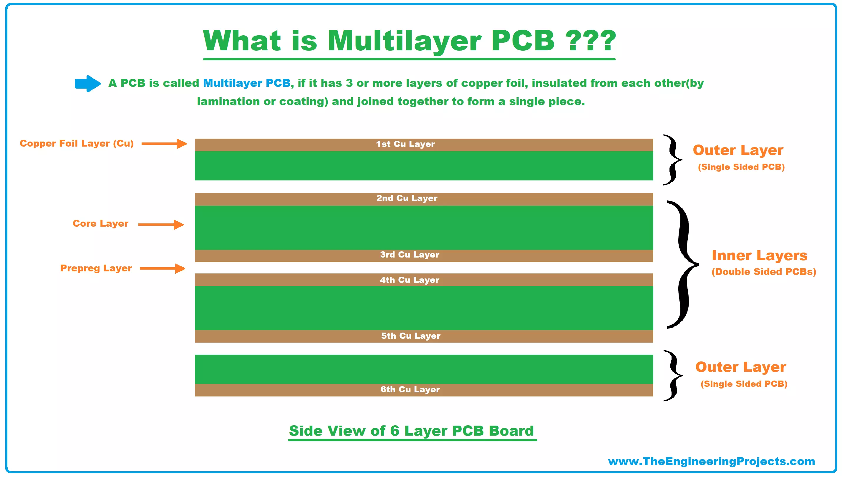
Hello Friends! I hope you all are well. Today, I am going
to share the 15th lecture in the PCB learning series. I am going to give
you a detailed overview of Multilayer PCB,
we will cover what is Multilayer PCB? & why do we need to use it?
We will also discuss its Construction, advantages, disadvantages, etc.
We have seen single-sided PCB
and double-sided PCB
in our previous posts, so go through them first.
Let's first have a look at the definition of PCB: PCB
is an abbreviation of the printed circuit board,
which comes with different copper conductive paths, traces & pads, incorporated on a single board to electrically connect different electronic components.
So, let's get started with What is MultiLayer PCB?
What is Multilayer PCB?
Initiall ...
Wave soldering is a widely used mass soldering process in the manufacturing of electronics, especially for through-hole elements and intricate technology printed circuit boards. In this method, a PCB is ignored, and a wave of melted solder permits solder joints to form on vulnerable part leads and pads at the same time. While wave soldering is effective and cost-efficient for high-volume manufacture, it is also liable to certain flaws if the method parameters, textiles, or patterns deliberation are not handled carefully.
Wave soldering defects in PCB assembly refer to general soldering flaws, such as spanning, defective solder, voids, and cold joints, that happen during the wave soldering process and can negatively affect the electrical execution, reliability, and long-term endurance of p ...
Hi Friends! Hope you’re well today. I welcome you on board. In this post today, I’ll walk you through the Top 10 Free Circuit Simulators for designing electronic projects. It's our 6th chapter in the PCB learning series.I am sharing this list of circuit simulators because you must simulate your circuit before designing its PCB. You’ll find scores of circuit simulators online. In this read, I’ve compiled the famous circuit simulators that help you design a circuit diagram for your electronics project. By designing these circuit simulations, you could text/debug your circuit. You can test it online before spending money on the real hardware. This will save you both time and money.
So, let’s get started:
Top 10 Free Circuit Simulators for Engineerin ...
To understand this section, we must know a little history. The history of the development of printed circuits is not as old as that of the industrial revolution, around 1950 is when the first PCBs began to be commercialized, however, in the early 1900s it was when the first attempts at PCB designs emerged.
The human being had the need to have electrical equipment that had a reduced size, before this the search began to replace the complex and extensive cable connections with electronic components.
It was on March 2, 1925, that Charles Ducas first filed a patent that included creating an electrical path directly on an insulating surface.
Technology has advanced and electronics are not left behind, as can be seen in the previous image, the first pr ...
Heat sinks are the electric routes for heat elimination from the PCB body. The digital electronic world is all about making devices compact and more powerful. This is possible only when the printed circuit boards (PCBs) are small enough to fit into the compact device. The increasing demand for power in low space comes with different challenges, of which the most crucial is the heat management of PCBs. The heat sinks are made of elements such as copper, aluminum, diamond, ceramic materials, graphite, etc., and play a crucial role in the thermal optimization of PCBs for optimal performance and long life. This comprehensive guide is about the basic introduction, heat transfer methods, key parameters, design considerations, and manufacturing techniques involved in the heat sink from the PCB po ...
Hello everyone and welcome to this article. Previously we have been discussing different types of PCB boards and for sure we have not exhausted everything. Today we are going to focus on a very important aspect of the PCB design which is the thermal characteristics of the PCB's working environment. Up to this moment, we have interacted with boards that work best in normal working conditions. But remember there are some working conditions, that have very harsh environment such as high temperatures. Let us take for example temperature in boilers or even electric heaters. Do you think normal FR-4 boards can survive in such temperatures? Don’t you think they will melt off if exposed to high thermal radiation? Your guess is as good as mine. For us to h ...
Hi readers! Hopefully, you are having a great day and exploring to learn something new. Heat is the silent killer in power electronics, and thermal vias are the unsung heroes that keep your circuit cool under pressure.
As electronic devices are miniaturized and powered with higher power, the amount of heat generated by high-speed and high-power devices has increased significantly. Proper thermal management is now one of the greatest challenges of modern-day PCB (Printed Circuit Board) design. Whether it is power supplies and LED light systems, or processors and RF modules, all electronic circuits are heat-generating. Unless treated carefully, such heat can cause degradation of components, reduced performance, signal instability, and even irreparable system damage.
To prevent such issues, ...
Hi Friends! Happy to see you around. Thank you for clicking this read. In this post today, I’ll document a detailed guide on the PCB fabrication process.
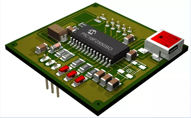
PCB is commonly used in modern electronics. If you uncover the TV set and have a look inside, you’ll find a printed circuit board, electrically connecting components on the board. There are copper traces incorporated on the board to electrically connect the components and provide the current flow from one part to another.
These printed boards make devices precise and compact that are capable of doing more functions than the devices where the end to end wiring is used.
Circuit boards are divided into three main types. Let’s discuss each type one by one so you can better understand the structure ...
JLCPCB (JiaLiChuang Co. Limited) is a worldwide PCB & PCBA Fabrication enterprise. It is a leading company in high-tech manufacturing products specializing in PCB and PCBA production. With over a decade of experience in PCB manufacturing JLCPCB has made over a million customers through online ordering by the customers of PCB manufacturing and PCBA production.
JLCPCB is a professional manufacturer of large-scale manufacturing of PCBs, well equipment, strict management, and superior quality. It deals with the production of all types of PCBs, Stencils, and SMT.
In this article, we are going to discuss widely how the company operates its ordering system of the PCBs by their customers for production through the online booking process.
JLCPCB SMT ...