Printed circuit board is a very important part of electronic devices. You will find them in all electronic appliances. To make a good quality PCB, it is very important to select high-grade materials. A PCB mainly consists of a NON-conductive material. Conductive lines are etched or printed on them.
PCB materials are mainly of 3 types.
FR-4TeflonMetal
Among these 3, FR-4 is the most common. This article will discuss all that you need to know about FR4 PCB Fabrication. We will discuss all about FR4. We will focus on its advantages.FR-4 Manufacturing
PCBway Fabricaton House manufactures high-quality FR4 PCBs. They can produce these PCBs really fast. The cost is also optimum. They are capable of making multi-layered FR4 PCBs.
PCBWay Fabrication H ...
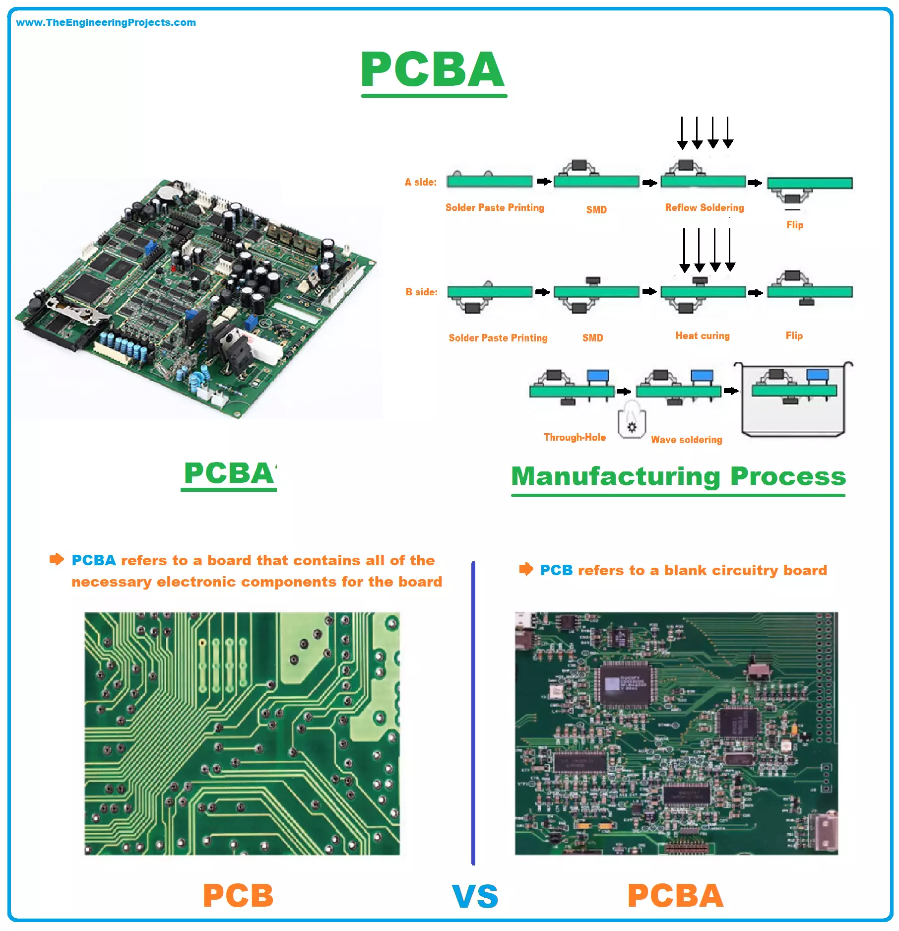
Hey Guys! Hope you’re well. I welcome you on board. In this post today, I’ll walk you through PCBA (Printed Circuit Board Assembly) in detail. It's our 4th tutorial in the PCB learning series.
In the 1st tutorial, we studied printed circuit board(PCB) in detail and learned that PCB provides physical support and electrical connection through conductive copper layers for the electronic components placed on the board. We have seen in our previous tutorials that when we place our PCB order on some PCB fabrication house, they provide us with a PCB board without electronic components. We have to solder the electronic components on the board. But now these PCB companies also offer a service to provide finished PCB boards with electronic components attach ...
Hi readers! I hope you’re having a great day and exploring something new. If you want a successful PCB, you should have a checklist of rules that are never broken. Today, the topic of our guide is Design Rule Check (DRC) Material and how to avoid common PCB layout mistakes.
In the area of electronic design, the foundation for the construction of all circuits and components is the Printed Circuit Board (PCB). Current device enhancements defined based on size reduction and enhanced complexity require PCB plans to reconcile electrical functionality, mechanical requirements, and assembly potential. A small layout mistake can cause short circuits, faulty connections, or manufacturing delays. This is where Design Rule Check (DRC) comes into play.
DRC is a computer-aided process that becomes pa ...
Hey there, I hope you are having a good day. Printed circuit boards (PCBs) are a popular topic in the electronic world and we also know that PCBs have revolutionized circuits. They not only provide a solid base but the material used in the PCBs helps the circuit to function properly by protecting the circuit from factors like external radiation. These are present in different materials that divide the working, stability, and reliability of the circuit. In recent years, there has been a significant change in the types and strength of PCBs and this depends on the materials used in the manufacturing of these boards. We are interested in studying the advanced materials used in the manufacturing of PCBs and knowing the right type of material for the right circuit.
...
Hi Friends! Hope you’re well today. I welcome you on board. Happy to see you around. In this post today, I’ll detail PCB Design Online Services for Engineering Students.
PCB designing is a crucial part of making some electrical projects. If you’re a student, you can leverage these services to design PCB online. You can design many PCB layouts for a single layer or multilayer PCB. Moreover, you can test simulation online and see how your design is working that you’re going to execute in real-time.
PCB Design Online Services for Engineering Students
You’ll find a list of online PCB design services. And I can understand, when you’re given a lot of options, it is very difficult to choose the best pick. The reason I have got you covered. In this post, ...
Hi Guys! Hope you’re well today. I welcome you on board. In this post, I’ll walk you through How to Install PCBWay Plugin for FreeCAD PCB Software.
Before we move further and help you with the installation of the plugin, let’s get a brief introduction to the FreeCAD software.
FreeCAD is a free and open-source parametric 3D modeler used to design real-life objects. With parametric modeling, you can easily modify your design and change its parameters. The tool is mainly used in mechanical engineering for product design and also proves to be handy in electrical engineering for electronic board designs. It supports Windows, Linux and macOS operating systems. Python programming language is primarily used to extend the overall functioning of the software.
Hope you’ve got an ...
Hi innovators! Wishing you the best day. One PCB defect, under the microscope, can spell the difference between a breakthrough and a disaster. Today, we will discuss PCB control test and how companies ensure its success.
Printed Circuit Boards (PCBs) are central to the current electronics era, and they are the power source of all forms of electronics: consumer electronics (like smartphones), life-saving medical equipment, aerospace control systems, and industrial automation. As the size of devices is steadily decreasing, their speed and efficiency, PCBs of high quality. Even a minor failure of a PCB could be disastrous to the products or costly recalls, or life-threatening in important applications.
To address such concerns, there is strict quality control (QC) in the production procedur ...
In the realm of PCB manufacturing, the Gerber file format plays an important role in the design and production processes. Understanding and inspecting these files are crucial to ensuring the accuracy and quality of the printed circuit board (PCB). JLCPCB is a leading PCB fabrication and assembly service provider. Fortunately, it offers an exceptional online tool. It is called the JLCPCB Online Gerber Viewer. It simplifies and enhances the inspection of PCB layouts. In this article, we will discuss the significance of Gerber files. We will explore the reasons for inspection. We will also showcase the powerful functionalities of JLCPCB's Online Gerber Viewer.
What is a Gerber file?
A Gerber file, named after the famous G ...
Hello Professional! Welcome to The Engineering Projects. We hope you are having a productive day. Today we'll talk about the building process of Printed Circuit Board with great efficiency and creativity.
It's hard-won to run an industrial company. What’s the reason? One is the bosses who have earned money quickly expand their business footprint not only focus on PCB, not delve into how to provide higher-quality PCB and more extreme customer service; also many bosses think more about engaging in financing and listing. How about JLCPCB?Yes, JLCPCB has planted into the PCB with all its heart, just keeping one aim: build the PCB best.
JLCPCB was founded in 2006, used to be the leading PCB company, now it is PCB industry big brother, who is highly appreciated and trusted by hardware fiel ...
Hi readers! I hope you are well and finding some thrilling advancement. In the high-speed electronic world where accuracy cannot be compromised and error is unthinkable, the Flying Probe Test is the unsung hero of PCB integrity. Today, the topic of our discourse is the Flying Probe Test and its use in PCB Fabrication.
In the complex realm of contemporary electronics, the dependability of a printed circuit board (PCB) can either make or destroy a product. With devices shrinking in size, speeding up in performance, and becoming increasingly feature-dense, the need for unflinching quality and accuracy in PCB manufacturing has grown stronger. Getting each trace, via, and connection perfectly manufactured is no longer a choice; it's a necessity. That's where Flying Probe Testing (FPT) comes in ...