


MCP4725 DAC Module Library for Proteus


Hello friends, I hope you all are doing great. Today, I am going to share the new MCP4725 DAC Module Library for Proteus, the first of the lab ICs in our University Lab series. A DAC, a digital-to-analog converter, does the opposite of the Arduino's analogRead: it takes a number and turns it into a real voltage. The Arduino UNO has no true DAC of its own; its analogWrite is only PWM, a fast on-off square wave. The MCP4725 adds a genuine 12-bit analog output over two I2C wires, and that is why it is everywhere in student labs: programmable reference voltages, sensor calibration, function generators, audio tones, motor and LED control, and closed-loop experiments.
MCP4725 DAC Module Library for Proteus
Latest version: V1.0 (November 2026, this tutorial)
Helping Tools
- Serial Monitor Advance: a serial terminal window for the UART of your board
- Serial Monitor Expert: the serial monitor with extra debugging tools
- LCD Library for Proteus V3.0: 16x2, 20x4 and I2C LCDs to show your readings
Our library brings it into Proteus on a small breakout board drawn at its true size, 18 x 13 mm. Every command, every byte of the read-back, the on-chip EEPROM with its write time, the power-down modes and the general call follow the datasheet, and the output follows the supply the way the real chip does. The pop-up shows the resistor string inside the DAC with its tap moving, the output buffer and the voltage over time. The demo is an Arduino that reads the DAC back, measures its linearity, stores a power-up value, switches the output off and on, and then plays a 251 Hz sine wave.
NOTICE: Our team has put a lot of effort into these small parts: the bodies, the animation and the pop-ups are all our own design, and you get them free. Your feedback is the fuel that keeps us going, so please tell us what you think in the comments below or in the MCP4725 board of our forum. And if our free libraries help you, you can buy us a coffee. So, let's get started with the MCP4725 DAC Module Library for Proteus:
What is the MCP4725?
The MCP4725 from Microchip is a single-channel, 12-bit, buffered voltage-output DAC in a tiny 6-pin SOT-23 package. Inside it there is a resistor string with 4096 taps, an output amplifier that drives the chosen tap to the VOUT pin rail to rail, an I2C interface, a power-on reset circuit, and a small EEPROM with its own charge pump, so the chip can remember a value with the power off.
| MCP4725 | |
|---|---|
| Resolution | 12 bits: codes 0 to 4095 |
| Output | VOUT = VDD x code / 4096, rail to rail, 1 Ω output impedance |
| Supply | 2.7 V to 5.5 V, 210 uA typical; VDD is also the reference |
| Speed | 6 us settling (typical), 0.55 V/us slew rate |
| Accuracy | DNL ±0.2 LSB typical; offset 0.02 %, gain -0.1 % of full scale typical |
| Interface | I2C at 100 kHz, 400 kHz or 3.4 MHz; address 1100 A2 A1 A0 |
| EEPROM | 14 bits (2 power-down bits + the 12-bit code), 25 ms write, 1 million cycles |
| Power-down | VOUT off, 1 kΩ, 100 kΩ or 500 kΩ to ground |
The Output Voltage
The MCP4725 has no reference pin: its supply is the reference. So the output is simply VOUT = VDD x code / 4096. On 5 V one step, one LSB, is 5 / 4096 = 1.22 mV; on 3.3 V it is 0.81 mV. Code 0 gives 0 V, code 2048 gives half the supply, and code 4095 gives one step below the supply. This makes it easy to use, but it also means that every wobble of the supply appears on the output: for precise voltages, the MCP4725 needs a clean supply.
The datasheet gives typical errors: an offset of 0.02 % of full scale at code 0 and a gain error of -0.1 % of full scale at code 4095. On 5 V that is 1 mV at the bottom and about 5 mV short at the top. Our model adds exactly those typical values (you can change them in the properties), so the numbers you measure look like a real part, not an ideal one.
The Address
The I2C address byte starts with the device code 1100, followed by A2, A1 and A0. A2 and A1 are fixed in the factory (00 unless ordered otherwise), and A0 comes from a pin. So a standard MCP4725 answers at 0x60, or 0x61 with A0 high. Our board has a jumper for A0 with a pull-down. Some breakouts use chips with other factory bits and answer at 0x62 or 0x63, so check your board.
The Commands
The MCP4725 understands three write commands, chosen by the top bits of the first byte after the address.
| Command | Bytes after the address | What it does |
|---|---|---|
| Fast mode (C2 C1 = 00) | 00 PD1 PD0 D11-D8, D7-D0 | updates the DAC register; repeat the pair for the next value |
| Write DAC register (010) | 010 x x PD1 PD0 x, D11-D4, D3-D0 xxxx | the same, in 3 bytes |
| Write DAC register and EEPROM (011) | 011 x x PD1 PD0 x, D11-D4, D3-D0 xxxx | also stores the code and PD bits in the EEPROM |
| Read | 5 bytes back | status, the DAC register (2 bytes), the EEPROM (2 bytes) |
Fast mode is the one for waveforms: after the address, every two bytes are a new output value, and the output updates at the acknowledge of the second byte. The 3-byte commands work the same way in groups of three, and a group that is cut short is ignored. The four codes starting with 1 are reserved, and the chip ignores them.
The Read-Back
Reading the chip returns five bytes. The first is a status byte: bit 7 is RDY/BSY (1 when no EEPROM write is running), bit 6 is POR, and bits 2 and 1 are the power-down bits. Bytes two and three hold the 12-bit DAC register, left-aligned. Bytes four and five hold the EEPROM: its two power-down bits and its 12-bit code. The datasheet shows the POR bit in the status byte without explaining it further; our model reads 1 while the chip is powered.
The EEPROM
Command 011 writes the EEPROM as well as the DAC register. The write takes 25 ms typically, 50 ms at most. During that time RDY/BSY reads 0 and the chip ignores every new write command, even a repeated one, so a sketch should poll the status before it writes again. At every power-on the chip loads the EEPROM into the DAC register, so the output starts at the stored value immediately; from the factory the EEPROM holds 800h, middle scale. The EEPROM lasts about a million write cycles, so store a power-up value only when it changes.
Power-Down and the General Call
The two PD bits switch the output off. With 01, 10 or 11 the amplifier stops, the chip draws only about 60 nA, and VOUT is connected to ground through 1 kΩ, 100 kΩ or 500 kΩ, so the load sees a known resistance instead of a floating pin. A new write with PD = 00 brings the output back. The MCP4725 also answers the I2C general call, address 00h: a second byte of 06h is a general call reset, which reloads the EEPROM into the DAC register just like a power-on, and 09h is a general call wake-up, which clears the PD bits and leaves the EEPROM alone.
Features of the MCP4725 DAC Module Library for Proteus
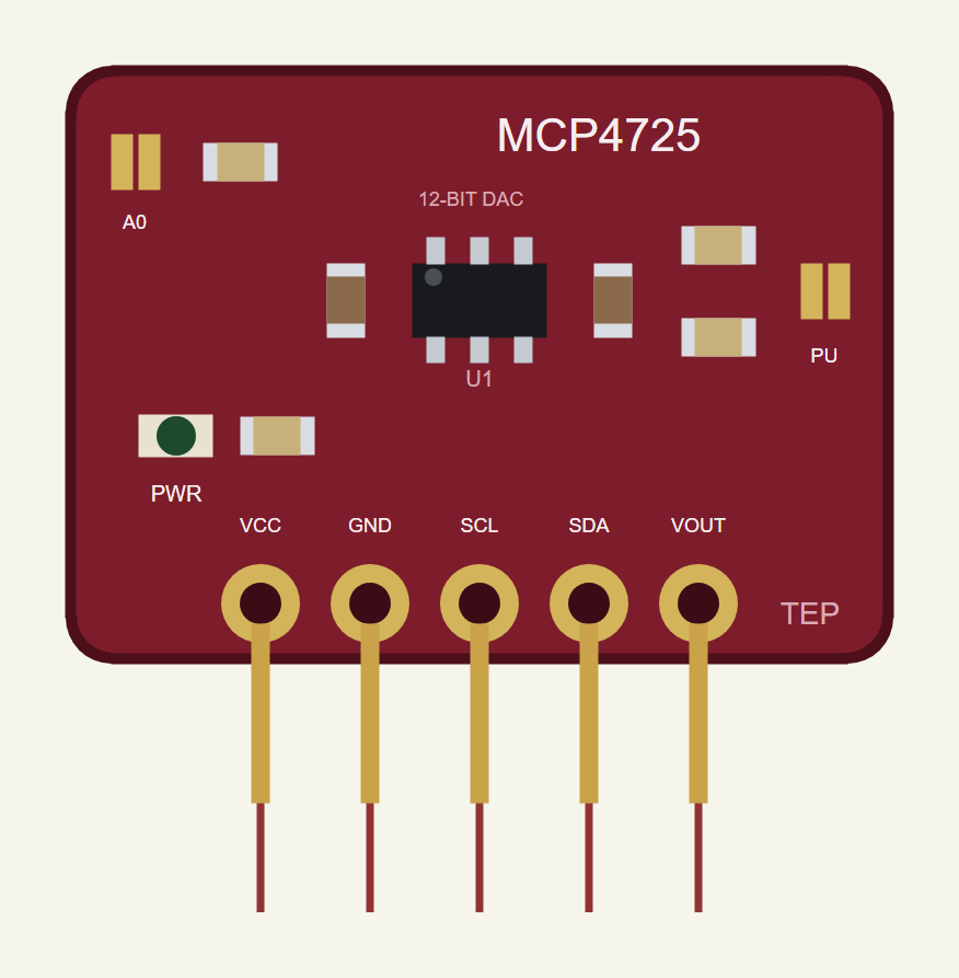
- A real breakout at true scale: 18 x 13 mm with the SOT-23-6 chip, the pull-ups, the A0 jumper and a PWR LED.
- Every command: fast mode, write DAC register and write DAC register and EEPROM, with repeats; reserved commands ignored.
- The 5-byte read-back: RDY/BSY, POR, the PD bits, the DAC register and the EEPROM.
- A real EEPROM: 25 ms writes with RDY/BSY, writes ignored meanwhile, the code loaded at power-on.
- Power-down and the general call: three output loads, reset and wake-up.
- A real output: VDD as the reference, the typical offset and gain errors, the 0.55 V/us slew rate.
- A pop-up: the resistor string and its tap, the buffer or the power-down load, VOUT over 20 or 500 ms, eight live values, graphs, an event log and a check page.
- A complete package: about 1.2 MB with the library, our Arduino UNO V4.0 and the demo, without the source code of the model.
The MCP4725 in Proteus
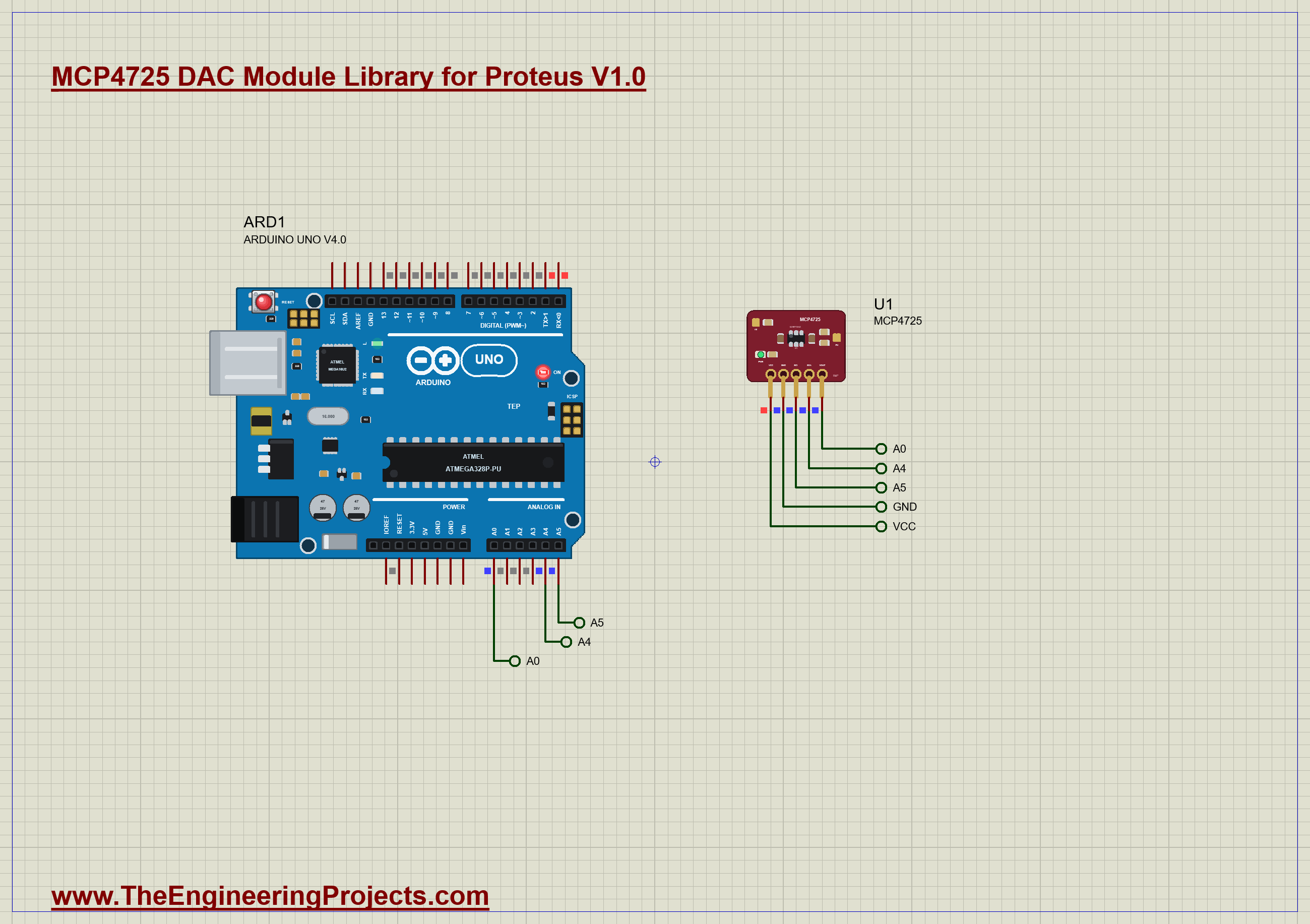
The device is MCP4725TEP in TEPMCP4725.LIB, under Lab ICs, with the prefix U and the model TEPMCP4725.DLL, a mixed model: VCC, GND and VOUT are analog, SCL and SDA digital. Search MCP4725 in Pick Devices. The header along the bottom edge has VCC, GND, SCL, SDA and VOUT on the 2.54 mm pitch. The MCP4725 runs happily from 5 V, so it connects straight to the UNO.
The Properties
| Property | What it does |
|---|---|
| A0 jumper (A0) | 0: address 0x60; 1: 0x61 |
| EEPROM (EEPROM) | the code in the EEPROM at power-up, 0 to 4095; 2048 (the factory value) by default |
| Offset error (OFFSET) | % of full scale at code 0; 0.02 (typical) by default |
| Gain error (GAIN) | % of full scale at code 4095; -0.1 (typical) by default |
Download MCP4725 DAC Module Library for Proteus
Click the button below to download MCP4725-DAC-Module-Library-for-Proteus-v1.0.zip (about 1.2 MB, without the source code of the models):
MCP4725 Library for Proteus V1.0- README.txt: installation, the demo, the wiring, troubleshooting and the limits.
- Proteus Library Files:
TEPMCP4725.LIBand ourArduinoV4TEP.LIB. - Proteus Model Files:
TEPMCP4725.DLLandTEPARDUINO.DLL. - Arduino Code: the demo sketch.
- Proteus Simulation: the demo project, its HEX file and copies of the DLLs.
No Proteus yet? Read How to Download and Install Proteus 7 and 8. New to libraries? Follow How to Install a New Library in Proteus.
How to Install MCP4725 DAC Module Library for Proteus
- Close Proteus and extract the whole zip file, for example to your Desktop.
- Copy the files from Proteus Library Files into the LIBRARY folder of Proteus.
- Copy the files from Proteus Model Files into the MODELS folder.
- Delete
TEPMCP4725.IDXfrom the LIBRARY folder if it is there. - Start Proteus, press P and search for MCP4725.
Demo: Testing the DAC and Playing a Sine Wave
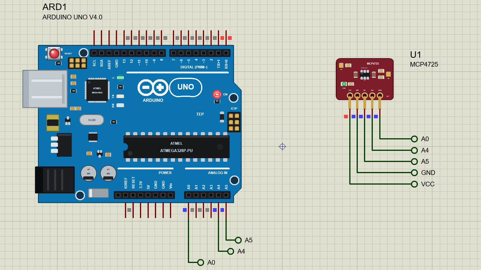
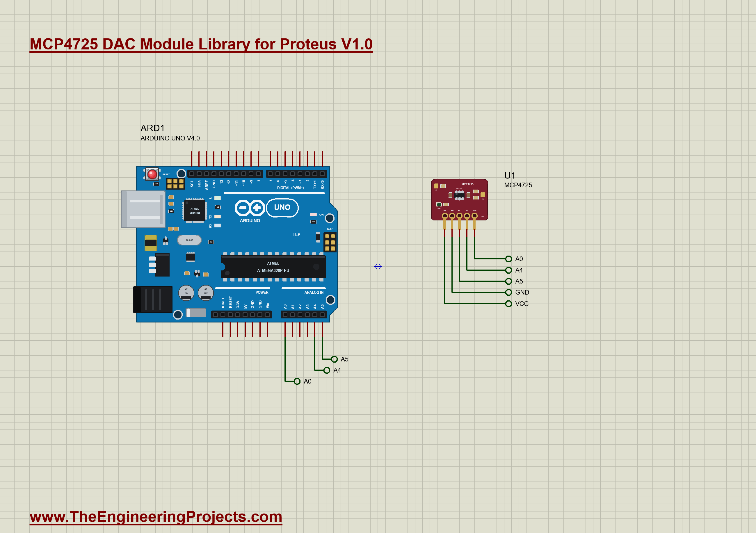
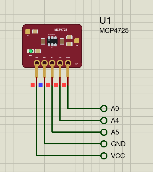
The demo is just the board and our Arduino UNO Library for Proteus V4.0, with its built-in monitor, the same window as our TEP Serial Monitor Advance for Proteus. VCC goes to the 5 V rail, SDA to A4, SCL to A5, and VOUT comes back into A0, so the UNO measures every voltage the DAC makes. The I2C bus runs at 400 kHz. Open MCP4725-DAC-ArduinoUnoV4.pdsprj.
The Sketch
The sketch uses only the Wire library, so every byte is visible. A fast-mode write is two bytes after the address: the power-down bits and the top four bits of the code, then the low eight bits:
void fastWrite(unsigned int code, byte pd) {                                   // 00 PD1 PD0 D11-D8, D7-D0
  Wire.beginTransmission(ADDR); Wire.write((pd << 4) | (code >> 8)); Wire.write(code & 0xFF); Wire.endTransmission();
}
Reading the chip back is a single five-byte request. The sketch keeps the status byte and rebuilds the two 12-bit codes from their halves:
void readBack() {                                                              // status, DAC register (2), EEPROM (2)
  Wire.requestFrom(ADDR, (byte)5);
  status = Wire.read();
  byte a = Wire.read(), b = Wire.read(), c = Wire.read(), d = Wire.read();
  dacCode = (a << 4) | (b >> 4);
  eepromCode = ((c & 0x0F) << 8) | d;
}
To store a value, it sends command 011 and then polls the RDY/BSY bit, timing how long the EEPROM takes:
  writeDacEeprom(1000);                                                        // 3. EEPROM
  unsigned long t0 = micros();
  do { readBack(); } while (!(status & 0x80));                                 // RDY/BSY
Then it tries a general call reset and a power-down with a general call wake-up, steps a 16-step staircase at 100 ms a step, and finally writes a 32-point sine table as fast as the bus allows for two seconds, counting the updates.
Run the Demo
Open the project and press Run. The demo runs about 5 simulated seconds, which Proteus ran in about two minutes on our PC. Click the board to open its pop-up; everything below is from that one run, the demo exactly as it ships.
Power-On and the Read-Back
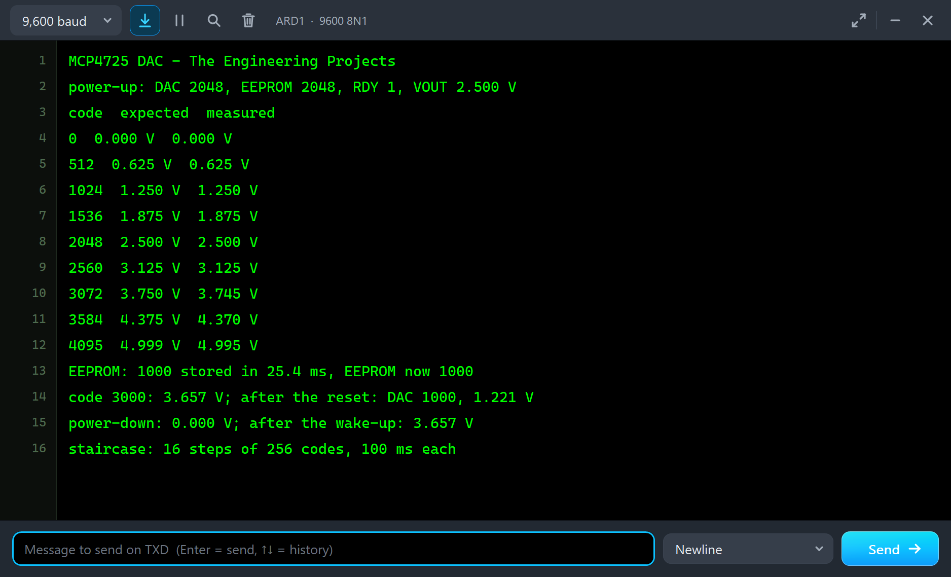
At 2 ms the board powers on and loads its EEPROM: code 2048, normal mode, so VOUT starts at middle scale before the sketch has done anything. The sketch reads the chip back as DAC 2048, EEPROM 2048, RDY 1, and measures VOUT at 2.500 V. The model shows 2.4985 V, the ideal 2.5 V plus the typical 1 mV offset minus half of the 5 mV gain error; the UNO's converter, with 4.9 mV steps, cannot see that difference.
Linearity
The sketch writes the codes 0, 512, 1024 and so on to 4095 and measures each one. The first six land exactly: 0.000, 0.625, 1.250, 1.875, 2.500 and 3.125 V. The last three read 3.745, 4.370 and 4.995 V against the ideal 3.750, 4.375 and 4.999 V: the typical -0.1 % gain error grows towards full scale and costs one step of the UNO's converter. A 12-bit DAC measured with a 10-bit ADC is limited by the ADC, which is a good lesson in itself.
The EEPROM, the Reset and Power-Down
The sketch stores code 1000 with command 011. The model holds RDY/BSY low for 25.0 ms; the sketch, polling the status byte, times 25.4 ms and reads the EEPROM back as 1000. Next it sets code 3000 with a fast write (3.657 V) and sends the general call reset: the DAC register reloads the EEPROM's 1000 and VOUT drops to 1.221 V. Then it writes 3000 with PD = 01: the output switches to 1 kΩ to ground and the UNO reads 0.000 V. The general call wake-up clears the PD bits and 3.657 V is back, because the code 3000 stayed in the DAC register all along.
The Staircase
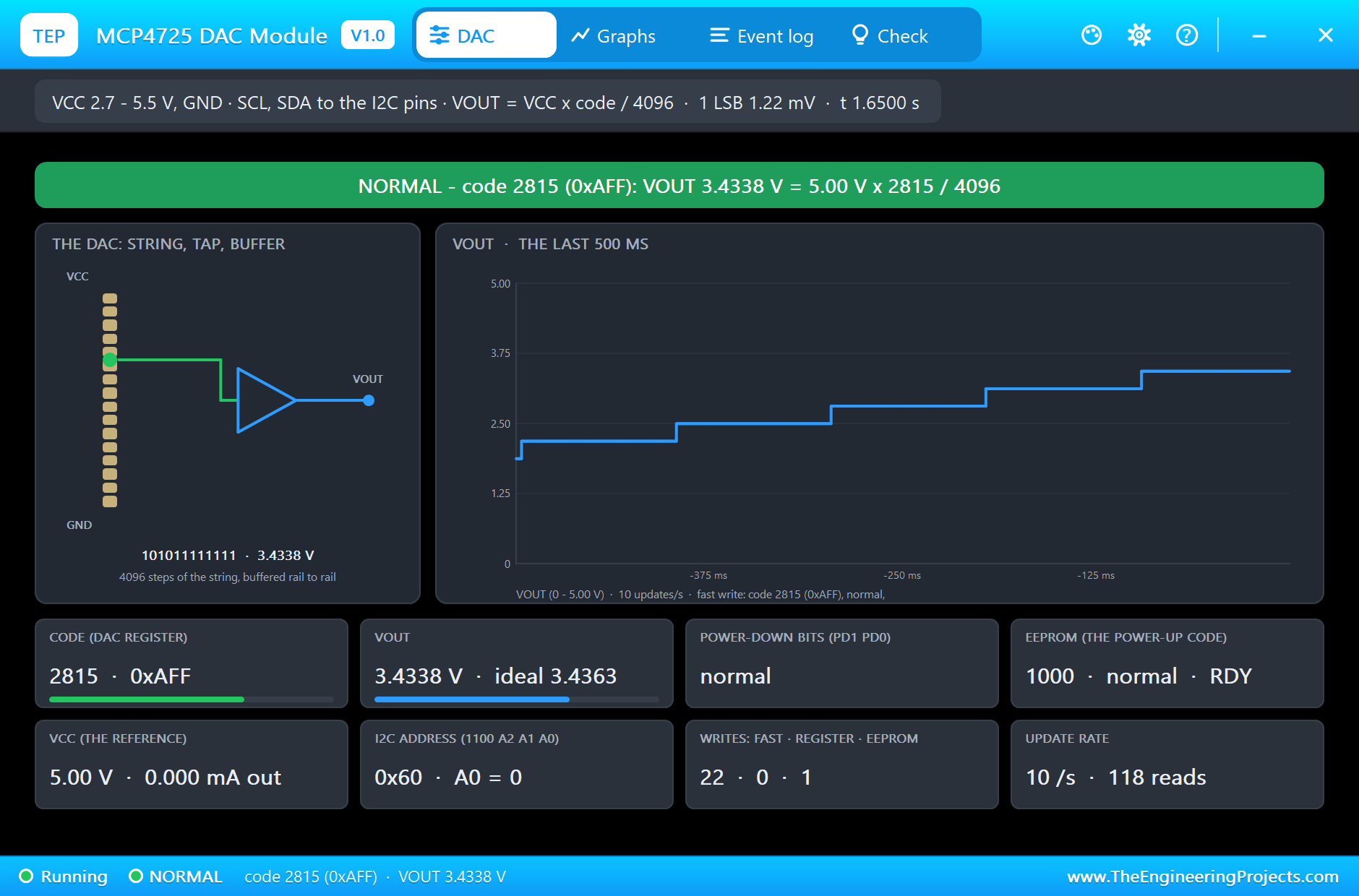
Next the sketch steps the output up in 16 steps of 256 codes, one every 100 ms. Because the updates are slow, the pop-up's scope switches to the last 500 ms, and the steps appear as a clean staircase. The capture below was taken at code 2815 (AFFh), 3.4338 V against an ideal 3.4363 V; the green tap sits about two thirds of the way up the resistor string.
A Sine Wave
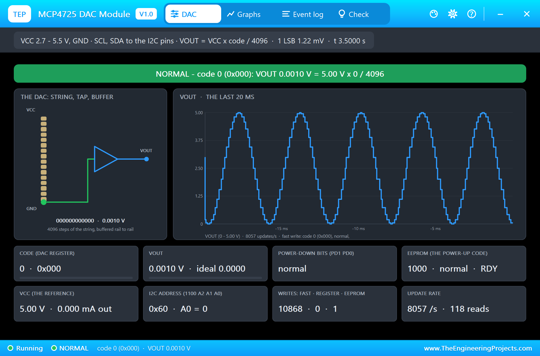
Finally the sketch writes its 32-point sine table with fast writes, one after another, for two seconds. Each update is the address byte and two data bytes on a 400 kHz bus, plus the Wire library's overhead. The result is 16105 updates in 2 s, 8053 updates per second, and with 32 points per cycle a 251.6 Hz sine. The scope switches to the last 20 ms and shows five cycles, each made of 32 visible steps, because a DAC holds each code until the next one arrives. In a real circuit a simple RC low-pass filter after VOUT smooths those steps into a clean sine.
The monitor then shows the whole story, from the power-up read-back to the sine's update rate.
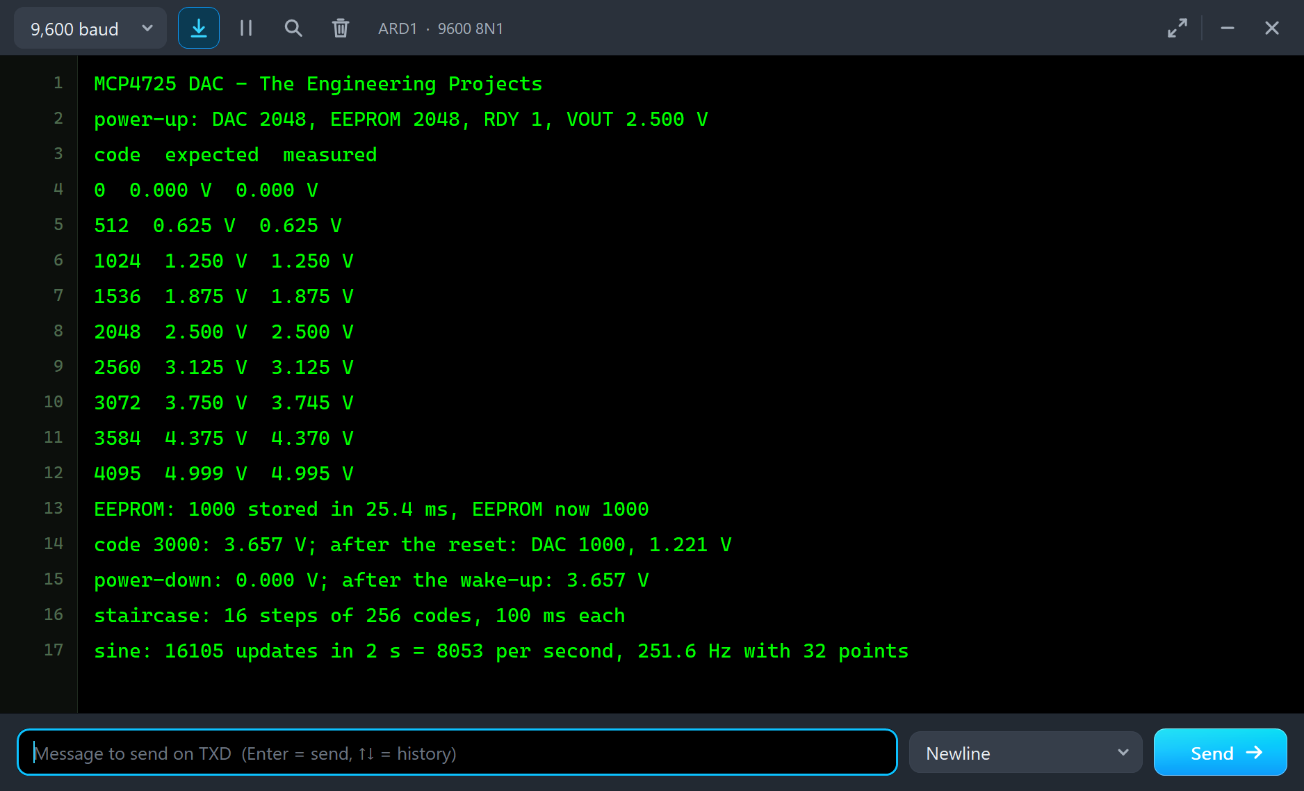
At the end the sketch writes 2048 again. In all, the chip received 16133 fast writes, 1 EEPROM write and 2 general calls, and answered 118 reads.
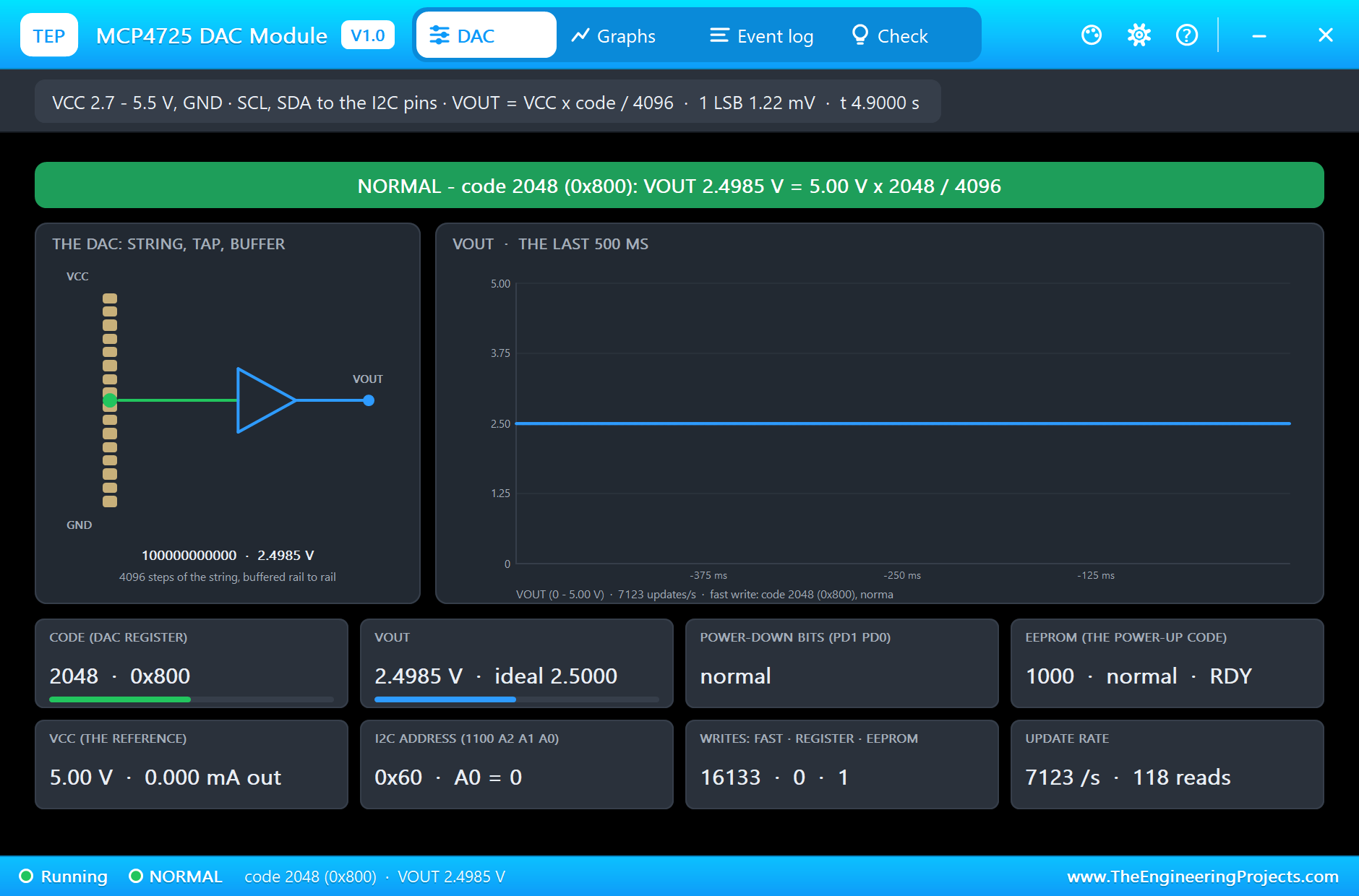
The Graphs, the Log and the Check Page
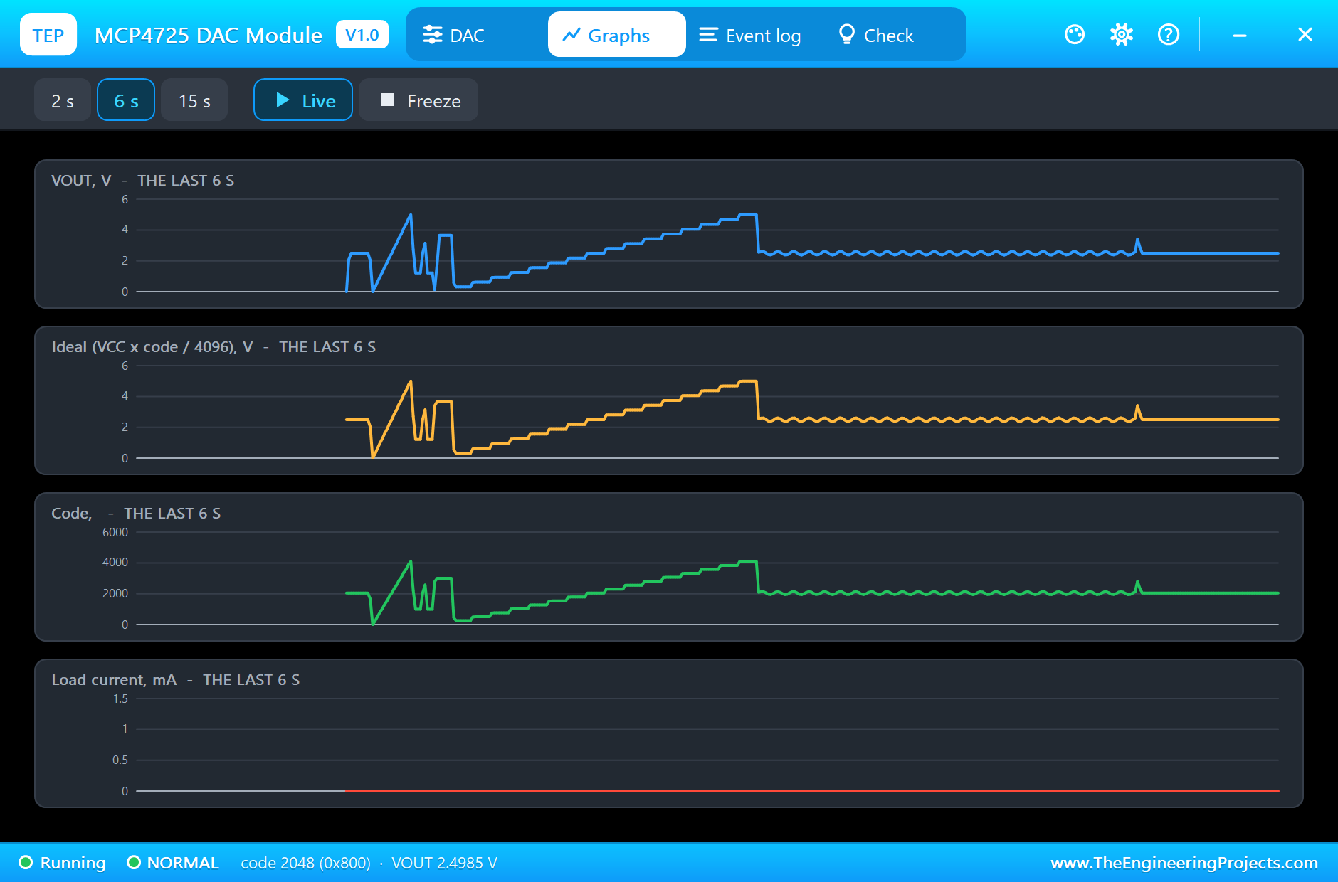
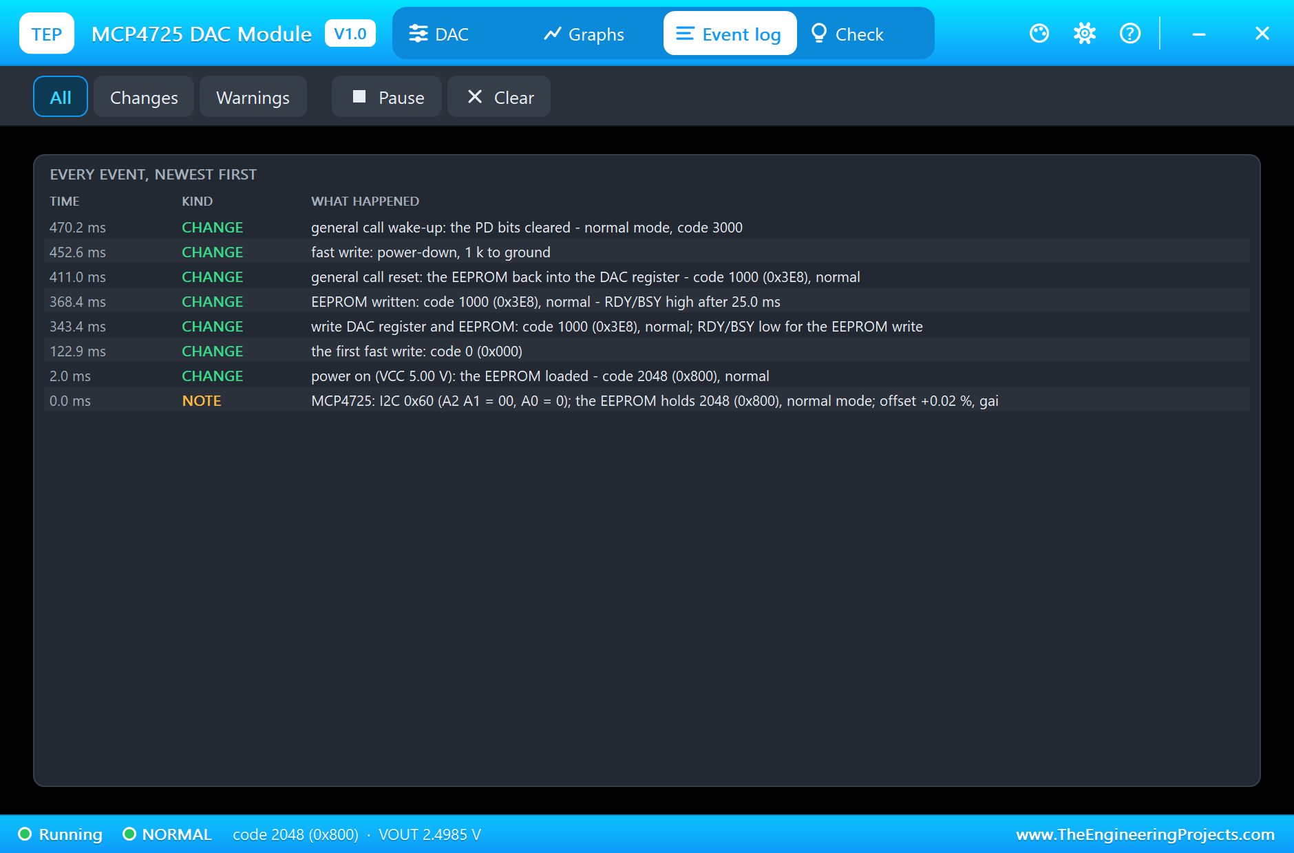
The Graphs page plots VOUT, the ideal value, the code and the load current over the last 2, 6 or 15 simulated seconds. The Event log keeps the power-on with the loaded code, the first fast write, the EEPROM write and its 25.0 ms, both general calls and the power-down; the thousands of fast writes are counted, not listed.
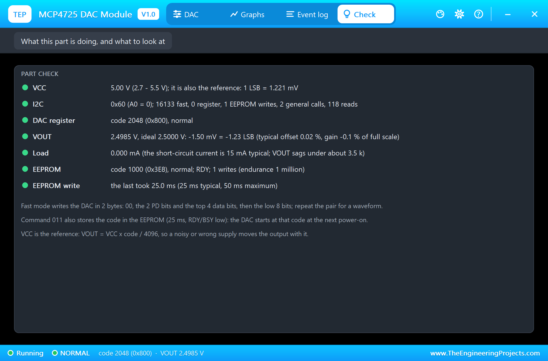
The Check page sums up the chip: VCC and the size of one step, the I2C traffic, the DAC register, VOUT's error against the ideal in millivolts and LSBs, the load current, the EEPROM and how long its last write took.
Try It Yourself
- Change the sine table to 64 points and see the frequency halve while the waveform gets smoother.
- Set the bus to 100 kHz and see how far the update rate falls.
- Write PD = 10 and 11 and measure VOUT with a 100 kΩ load: see the power-down resistors at work.
- Store a different value in the EEPROM, stop and restart the simulation: the DAC starts at it.
- Set GAIN to 0 and OFFSET to 0 for an ideal DAC, and compare the linearity table.
- Use two boards on one bus, one with A0 at 1, as a two-channel DAC.
Ideas to Extend the Demo
- Build a function generator with sine, triangle and square waves chosen from the serial monitor.
- Make a programmable reference for a comparator or an op-amp circuit.
- Close a loop: let the DAC drive an LED and a light sensor read it back.
- Play a short melody by changing the sine's step rate.
Your Own Sketches
The demo sketch is in the zip file, and you can change it in the Arduino IDE. New to Arduino? Start with our Arduino Tutorial for Beginners. Export the compiled binary, and set the UNO's PROGRAM property to the new file. Our guide on How to get the HEX file from Arduino shows you where the file ends up.
Things to Know Before Using a Real Module
- The supply is the reference: a noisy USB supply puts its noise on VOUT; use a clean or regulated supply for precise voltages.
- Mind the load: the output can drive about 25 mA at most and sags under about 3.5 kΩ; buffer it with an op-amp for heavier loads.
- Save the EEPROM: about a million writes; store a power-up value now and then, never in a loop.
- Check the address: 0x60 / 0x61 here, but some boards answer at 0x62 / 0x63.
Troubleshooting
- NO SUPPLY: VCC is missing or under the 2 V power-on threshold.
- "no MCP4725 at 0x60": SDA and SCL swapped or not connected, or the A0 property is 1 (0x61).
- VOUT stays at 0: the PD bits are set; write with PD = 00 or send the general call wake-up.
- Writes are ignored for a moment: an EEPROM write is running; poll RDY/BSY first.
- VOUT is a little off: the reference is VCC, so measure VCC; the typical offset and gain errors are also in the model.
- The part is not simulated:
TEPMCP4725.DLLis missing from MODELS and from the project folder.
Limitations of the Simulation
- INL and DNL, glitches and noise are not modelled; the output is the ideal value plus the typical offset and gain errors.
- The output's current limit and its sag under heavy loads are not modelled; a load current over 15 mA is reported on the Check page.
- The I2C high-speed mode (3.4 MHz) and the bus timing limits are not checked.
- Arduino is a name of Arduino and MCP4725 of Microchip; this library is not made or endorsed by Arduino, Labcenter or Microchip.
- Tested in Proteus 8.5 in November 2026 (the demo as shipped). Proteus 7 is not supported.
So, that was all about the MCP4725 DAC Module Library for Proteus. I hope it helps you build your analog-output project on your own PC first: a real 12-bit voltage from two I2C wires, an EEPROM that remembers it, and a sketch that tests every feature byte by byte. If you have any questions, ask in the comments and I will help you out. Till the next tutorial, take care and have fun!

Comments
0