


MCP3008 8-Channel ADC Library for Proteus


Hello friends, I hope you all are doing great. Today, I am going to share the new MCP3008 8-Channel ADC Library for Proteus, the second of the lab ICs in our University Lab series. An ADC, an analog-to-digital converter, turns a voltage into a number. The MCP3008 does it for eight inputs at once, with 10 bits, over a four-wire SPI bus, and it is the standard way to give a board without analog inputs, such as the Raspberry Pi, its analog pins, or to give an Arduino more of them. Students meet it in sensor labs, data loggers, joystick and potentiometer projects, and in every course that teaches how SPI works.
MCP3008 8-Channel ADC Library for Proteus
Latest version: V1.0 (November 2026, this tutorial)
Helping Tools
- Serial Monitor Advance: a serial terminal window for the UART of your board
- Serial Monitor Expert: the serial monitor with extra debugging tools
- LCD Library for Proteus V3.0: 16x2, 20x4 and I2C LCDs to show your readings
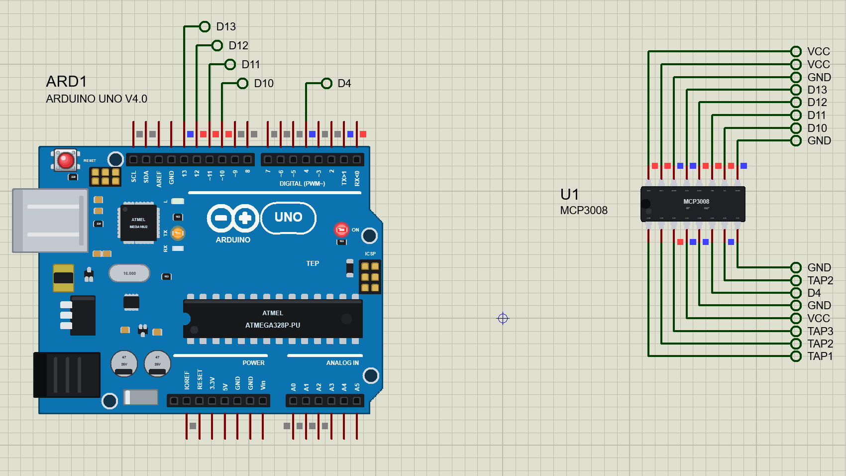
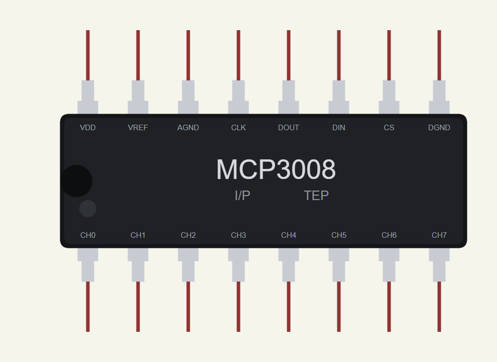
Our library brings the chip itself into Proteus: the 16-pin DIP drawn at its true size, 19.3 x 6.35 mm. The model converts exactly as the datasheet describes, eight single-ended inputs or four pseudo-differential pairs, and it speaks the MCP3008's serial protocol bit by bit: the start bit, the channel bits, the null bit and the ten result bits. It checks the clock against its limit and the differential inputs against their range, and the pop-up draws the last SPI transfer as a timing diagram, clock by clock. The demo is an Arduino reading a resistor ladder, a differential pair and one of its own pins.
NOTICE: Our team has put a lot of effort into these small parts: the bodies, the animation and the pop-ups are all our own design, and you get them free. Your feedback is the fuel that keeps us going, so please tell us what you think in the comments below or in the MCP3008 board of our forum. And if our free libraries help you, you can buy us a coffee. So, let's get started with the MCP3008 8-Channel ADC Library for Proteus:
What is the MCP3008?
The MCP3008 from Microchip is a 10-bit successive-approximation A/D converter with an eight-channel input multiplexer, a sample-and-hold, and an SPI interface. A successive-approximation converter finds the result one bit at a time, from the most significant bit down, comparing the held input with a DAC inside; that is why the MCP3008 can send each bit out the moment it has decided it.
| MCP3008 | |
|---|---|
| Resolution | 10 bits: codes 0 to 1023 (000h to 3FFh), straight binary |
| Inputs | 8 single-ended or 4 pseudo-differential pairs |
| Speed | 200 ksps at 5 V, 75 ksps at 2.7 V |
| Clock | up to 3.6 MHz at 5 V, 1.35 MHz at 2.7 V |
| Accuracy | INL and DNL ±1 LSB maximum |
| Supply | 2.7 V to 5.5 V; 425 uA typical converting, 5 nA typical in standby |
| Reference | VREF from 0.25 V to VDD sets the input range |
| Package | PDIP-16 or SOIC-16; SPI modes 0,0 and 1,1 |
The Result
The result is code = 1024 x VIN / VREF, rounded down. With VREF at 5 V, one step, one LSB, is 5 / 1024 = 4.88 mV; with VREF at 2.5 V it is 2.44 mV, so a lower reference gives finer steps for small signals, at the price of a smaller range. An input at or above VREF reads 1023, and an input at 0 V reads 0. Note that a code stands for a whole step: code 433 means anything from 433 to 434 LSB. Multiplying the code by the LSB gives the bottom of that step, and adding half an LSB gives its middle.
Single-Ended and Pseudo-Differential
In single-ended mode each channel is measured against AGND. In pseudo-differential mode the channels pair up, CH0 with CH1, CH2 with CH3 and so on, and the chip measures the difference between them. One of the pair is IN+ and the other IN-, and the D0 bit decides which is which. The word "pseudo" matters: IN- is only meant to wander within 100 mV of ground, to cancel a little common-mode noise. It is not a full differential input that can sit anywhere. If IN+ is at or below IN-, the result is 0.
The Pins
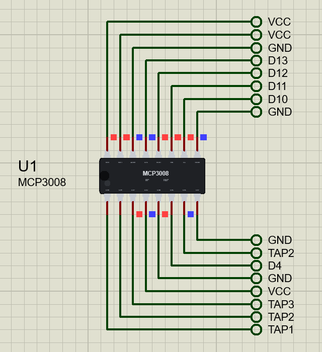
On the PDIP-16, pins 1 to 8 are CH0 to CH7. On the other side, pin 9 is DGND, 10 CS/SHDN, 11 DIN, 12 DOUT, 13 CLK, 14 AGND, 15 VREF and 16 VDD. Our drawing lies on its side with the notch on the left, so CH0 to CH7 run along the bottom and VDD to DGND along the top, with the names printed small inside the edges.
The SPI Protocol, Bit by Bit
The MCP3008's protocol is short, and it is worth knowing exactly. CS goes low to begin. The first clock with DIN high is the start bit. The next four clocks bring SGL/DIFF (1 for single-ended) and the three channel bits D2 D1 D0. The chip starts to sample the input on the fourth rising edge after the start bit and stops on the falling edge of the fifth, where it puts out a low null bit. On the next ten falling edges it sends the result, B9 to B0, most significant bit first. If the clock keeps running, it sends the result again least significant bit first, then zeros. Before the null bit and after CS rises, DOUT is high-impedance. CS must go high between conversions, and once after power-up before the first one.
| Clock (from the start bit) | DIN | DOUT |
|---|---|---|
| 0 | start bit (1) | Hi-Z |
| 1 | SGL/DIFF | Hi-Z |
| 2, 3, 4 | D2, D1, D0 | Hi-Z (the sample starts at 4) |
| 5 | don't care | null bit (0), the sample ends |
| 6 to 15 | don't care | B9 to B0 |
| 16 and on | don't care | B1 to B9 (LSB first), then zeros |
An Arduino's SPI hardware sends whole bytes, so the usual trick, the one in the datasheet, is to send seven zeros before the start bit. The first byte is then 01h; the second carries SGL/DIFF and D2 D1 D0 in its top four bits and brings back the null bit and B9 and B8 in its lowest bits; the third brings back B7 to B0. Three bytes, 24 clocks, one conversion.
Speed and the Clock Limit
The sample lasts only 1.5 clocks. In that time an internal 20 pF capacitor must charge through a 1 kΩ switch, plus whatever resistance the source has, to within a fraction of an LSB. That is where the clock limit comes from: 3.6 MHz at 5 V and 1.35 MHz at 2.7 V. A faster clock leaves the capacitor short of its final voltage, and a high-impedance source makes it worse. Our model measures the clock of every transfer, warns when it is over the limit for the present supply, and says so on the Check page.
Features of the MCP3008 8-Channel ADC Library for Proteus
- The real chip at true scale: the PDIP-16, 19.3 x 6.35 mm, with its real pinout.
- The datasheet's conversion: code = 1024 x VIN / VREF, 8 single-ended inputs or 4 pseudo-differential pairs.
- The whole protocol: the start bit, SGL/DIFF and D2 D1 D0, the null bit, MSB first, LSB first, zeros and Hi-Z; CS and standby.
- Checks: the clock against 3.6 MHz at 5 V (1.35 MHz at 2.7 V), IN- against its 100 mV, VREF against 0.25 V to VDD.
- A timing diagram: the pop-up draws the last transfer clock by clock, with the start bit, the control bits, the null bit and B9 to B0 labelled.
- A pop-up: the eight inputs as bars with their codes, eight live values, graphs, an event log and a check page.
- A complete package: about 1.2 MB with the library, our Arduino UNO V4.0 and the demo, without the source code of the model.
The MCP3008 in Proteus
The device is MCP3008TEP in TEPMCP3008.LIB, under Lab ICs, with the prefix U and the model TEPMCP3008.DLL, a mixed model: the eight inputs, VDD, VREF, AGND and DGND are analog; CLK, DIN and CS are digital inputs and DOUT a digital output. Search MCP3008 in Pick Devices. It has one property, VMIN, the supply below which the Check page warns (2.7 V).
Download MCP3008 8-Channel ADC Library for Proteus
Click the button below to download MCP3008-8-Channel-ADC-Library-for-Proteus-v1.0.zip (about 1.2 MB, without the source code of the models):
MCP3008 Library for Proteus V1.0- README.txt: installation, the demo, the wiring, troubleshooting and the limits.
- Proteus Library Files:
TEPMCP3008.LIBand ourArduinoV4TEP.LIB. - Proteus Model Files:
TEPMCP3008.DLLandTEPARDUINO.DLL. - Arduino Code: the demo sketch.
- Proteus Simulation: the demo project, its HEX file and copies of the DLLs.
No Proteus yet? Read How to Download and Install Proteus 7 and 8. New to libraries? Follow How to Install a New Library in Proteus.
How to Install MCP3008 8-Channel ADC Library for Proteus
- Close Proteus and extract the whole zip file, for example to your Desktop.
- Copy the files from Proteus Library Files into the LIBRARY folder of Proteus.
- Copy the files from Proteus Model Files into the MODELS folder.
- Delete
TEPMCP3008.IDXfrom the LIBRARY folder if it is there. - Start Proteus, press P and search for MCP3008.
Demo: Eight Channels, a Differential Pair and a Speed Test
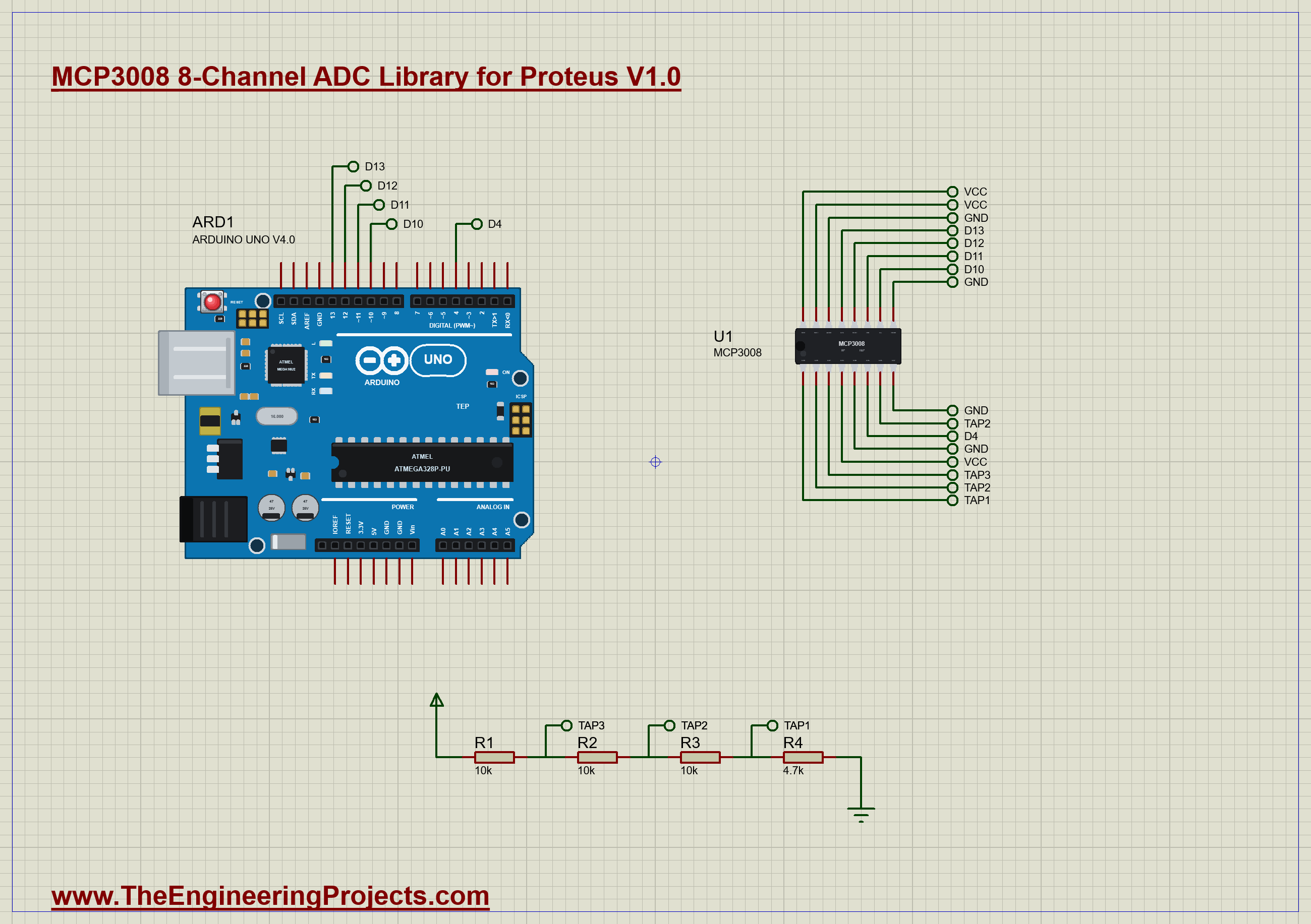
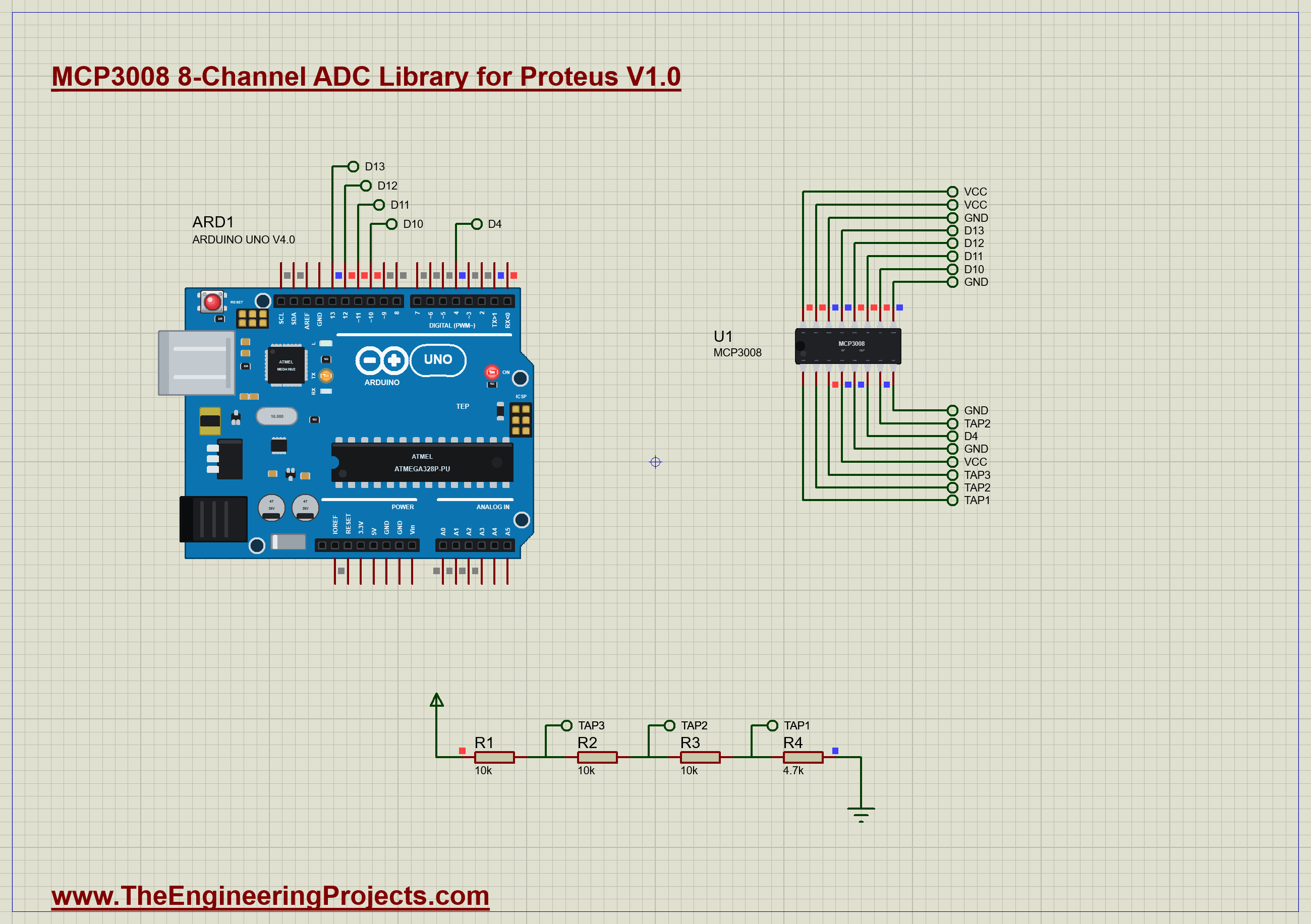
The demo has our Arduino UNO Library for Proteus V4.0 with its built-in monitor, the same window as our TEP Serial Monitor Advance for Proteus, the MCP3008, and four resistors. VDD and VREF go to 5 V, AGND and DGND to ground, and the SPI pins to the UNO: CS to D10, DIN to D11, DOUT to D12 and CLK to D13. A ladder of 10 kΩ, 10 kΩ, 10 kΩ and 4.7 kΩ from 5 V to ground gives three test voltages, 3.559 V, 2.118 V and 0.677 V, chosen to fall in the middle of a code rather than on a boundary. CH0, CH1 and CH2 read the three taps, CH3 is on 5 V, CH4 on ground, CH5 on the UNO's D4, and CH6 and CH7 form a pair, 2.118 V and ground. Open MCP3008-ADC-ArduinoUnoV4.pdsprj.
The Sketch
The whole conversation with the chip is one small function. It drops CS, sends the three bytes described above and puts the ten result bits together from the last two replies:
int readAdc(byte sgl, byte channel) {
  digitalWrite(CS, LOW);
  SPI.transfer(0x01);                                                          // 7 leading zeros, the start bit
  byte hi = SPI.transfer((sgl << 7) | (channel << 4));                         // SGL/DIFF D2 D1 D0 in; the null bit, B9, B8 out
  byte lo = SPI.transfer(0x00);                                                // B7 - B0
  digitalWrite(CS, HIGH);
  return ((hi & 0x03) << 8) | lo;
}
The bus runs in SPI mode 0 at 1 MHz. The sketch reads all eight channels single-ended, sets D4 high and reads CH5 again, reads the pair both ways round, and times 1000 conversions of CH1. Then, on purpose, it makes one conversion with the clock at 4 MHz, over the limit:
  SPI.endTransaction();                                                        // 4. too fast
  SPI.beginTransaction(SPISettings(4000000, MSBFIRST, SPI_MODE0));
  Serial.print("at 4 MHz: CH1 = "); Serial.println(readAdc(1, 1));
After a three-second pause it flips D4 every 250 ms and prints CH5.
Run the Demo
Open the project and press Run. The demo runs 6 simulated seconds, which Proteus ran in a little over two minutes on our PC. Click the chip to open its pop-up; everything below is from that one run, the demo exactly as it ships.
Eight Channels
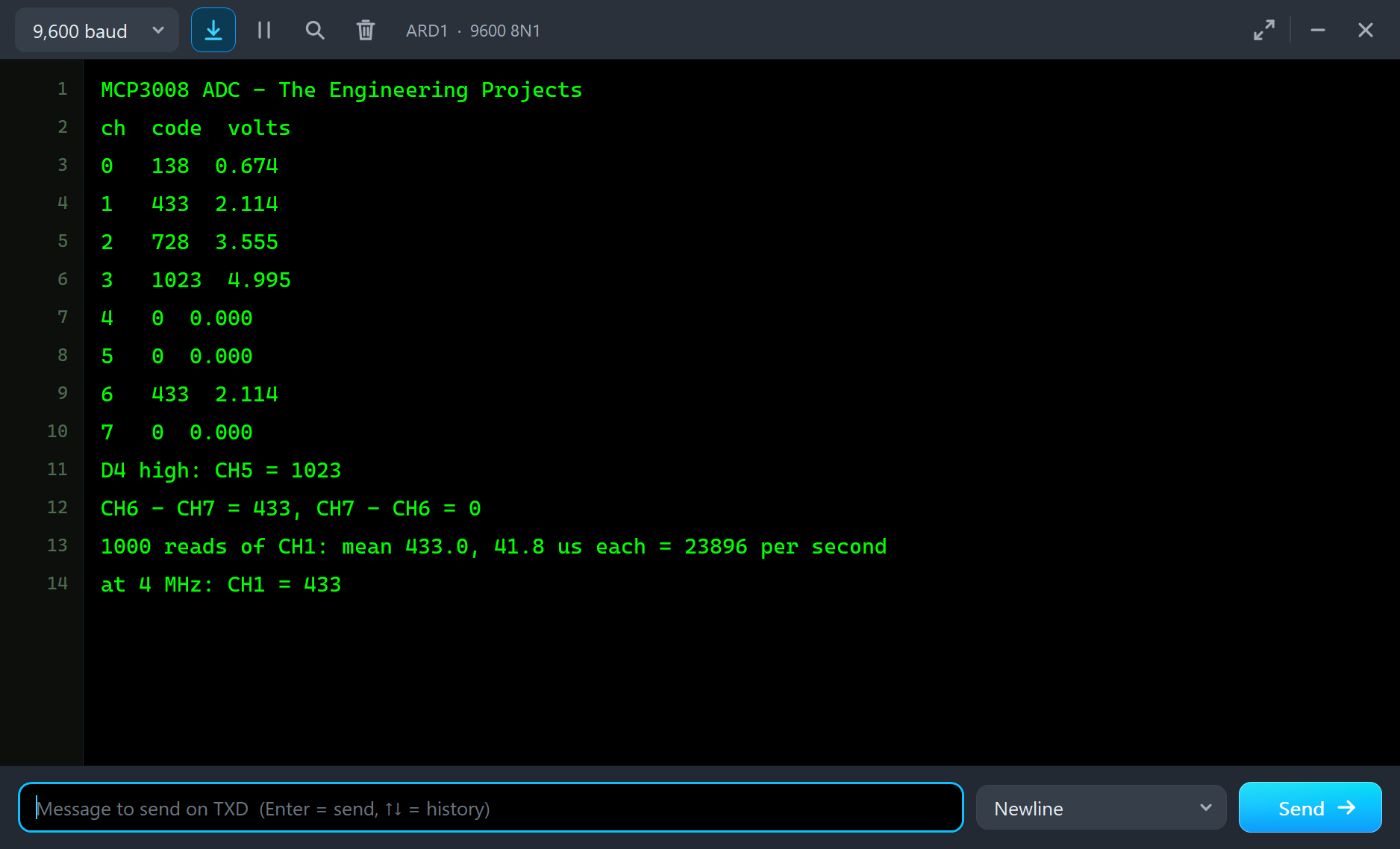
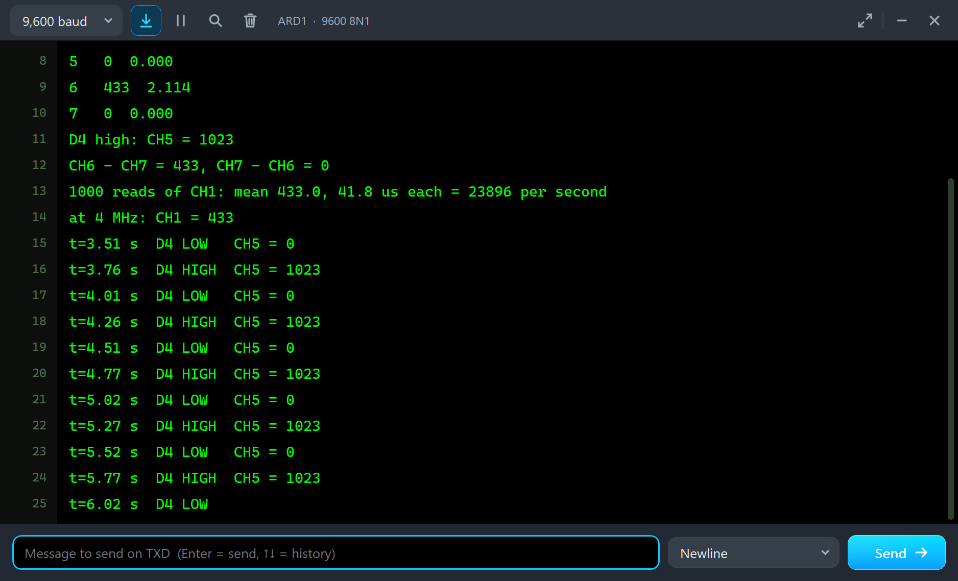
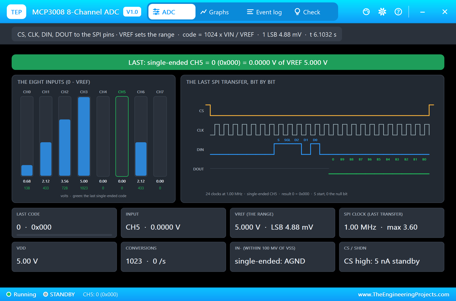
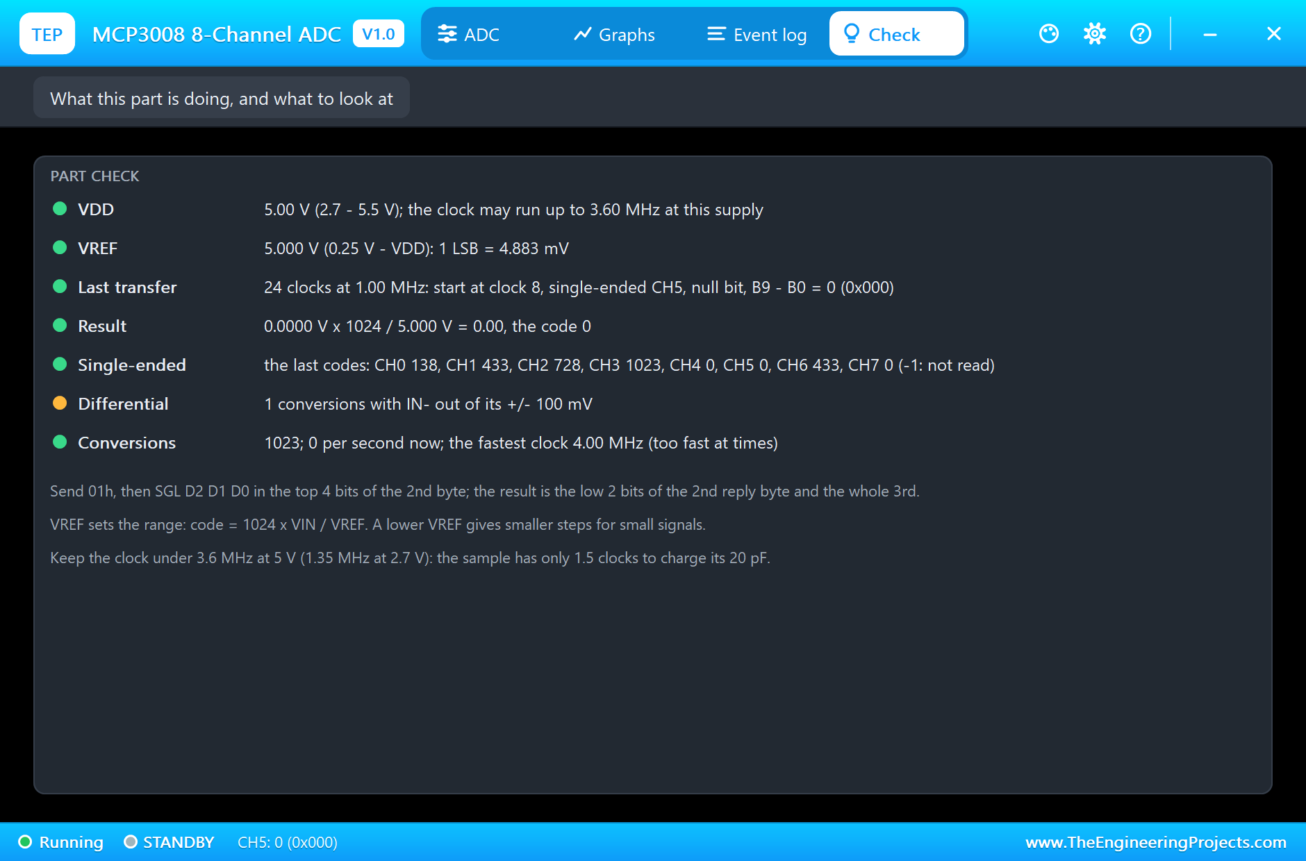
The first conversion comes at 65.8 ms: CH0, 138 (08Ah), from 0.6772 V, with the clock measured at 1.00 MHz. The full scan reads CH0 138, CH1 433, CH2 728, CH3 1023, CH4 0, CH5 0, CH6 433 and CH7 0. Check them against the formula: 1024 x 2.1182 / 5 = 433.8, so 433; 1024 x 3.559 / 5 = 728.9, so 728; and 5 V on CH3 is the top of the range, 1023. The sketch prints the voltages as code x 5 / 1024, which gives 0.674, 2.114 and 3.555 V: each a little under the real input, because that formula gives the bottom of the code's 4.88 mV step. With D4 high, CH5 reads 1023.
The Differential Pair
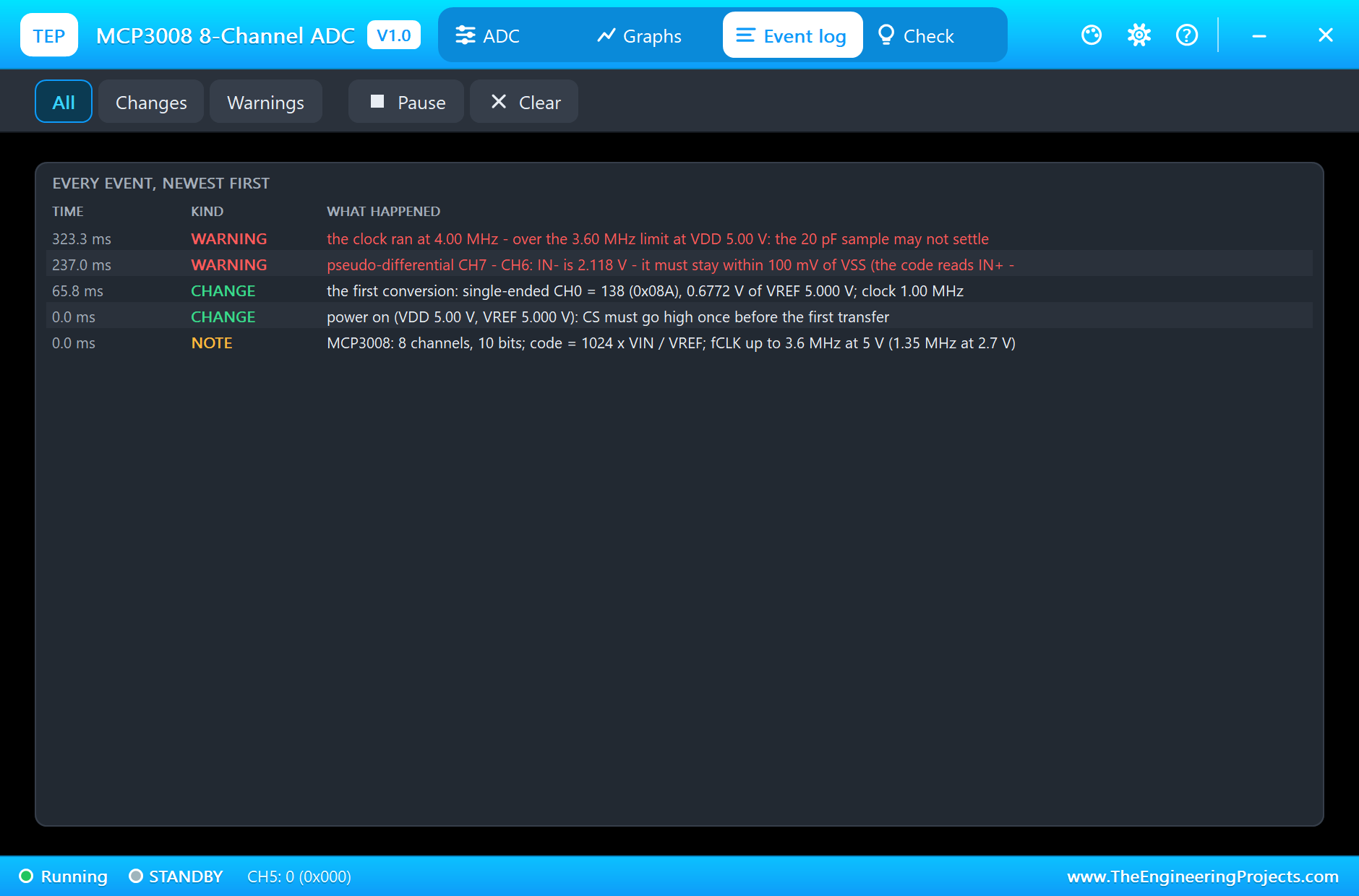
CH6 - CH7, with CH6 as IN+ at 2.118 V and CH7 as IN- at 0 V, reads 433, the same as CH6 alone, because IN- is at ground. The other way round, CH7 - CH6, IN+ is at 0 V and IN- at 2.118 V. IN+ is below IN-, so the result is 0, and the model warns in its log that IN- was 2.118 V, far outside its 100 mV. On a real chip that conversion would be out of specification.
Speed
1000 conversions of CH1 average exactly 433.0 and take 41.8 us each: 23896 conversions per second. The 24 clocks at 1 MHz account for 24 us; the rest is the Arduino's SPI calls, the CS pin and the loop. The MCP3008 itself could go much faster: at 3.6 MHz and its full 200 ksps, a conversion takes 5 us.
Over the Clock Limit
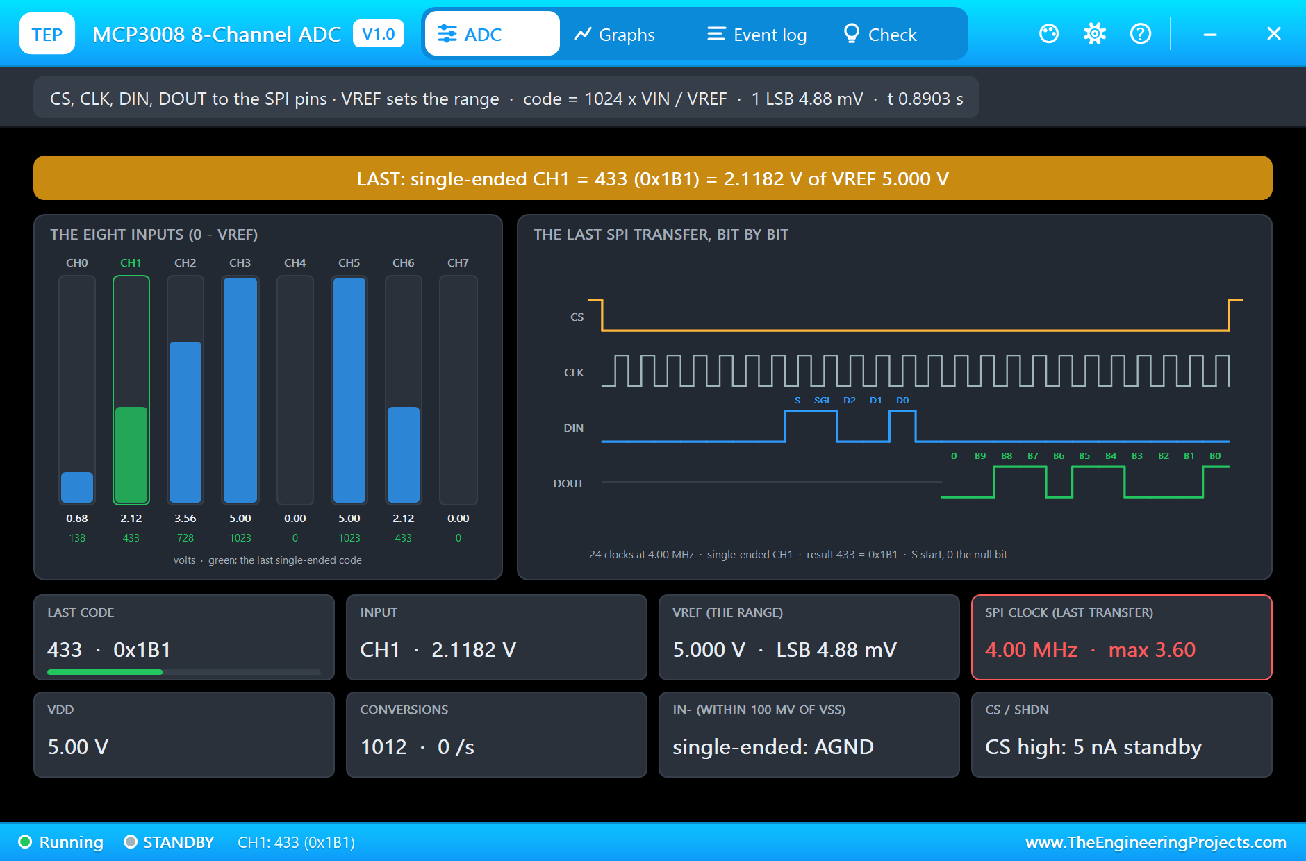
The conversion at 4 MHz still reads 433, because our model computes the code from the sampled voltage. But it measures the clock at 4.00 MHz, over the 3.60 MHz limit at 5 V, so the banner turns amber, the clock tile turns red and the log records the warning. The timing diagram shows the whole transfer: 24 clocks, DIN low for seven clocks, the start bit, SGL high, D2 D1 D0 = 001 for CH1, DOUT high-impedance until the null bit, and then 0110110001, which is 433.
Following a Pin
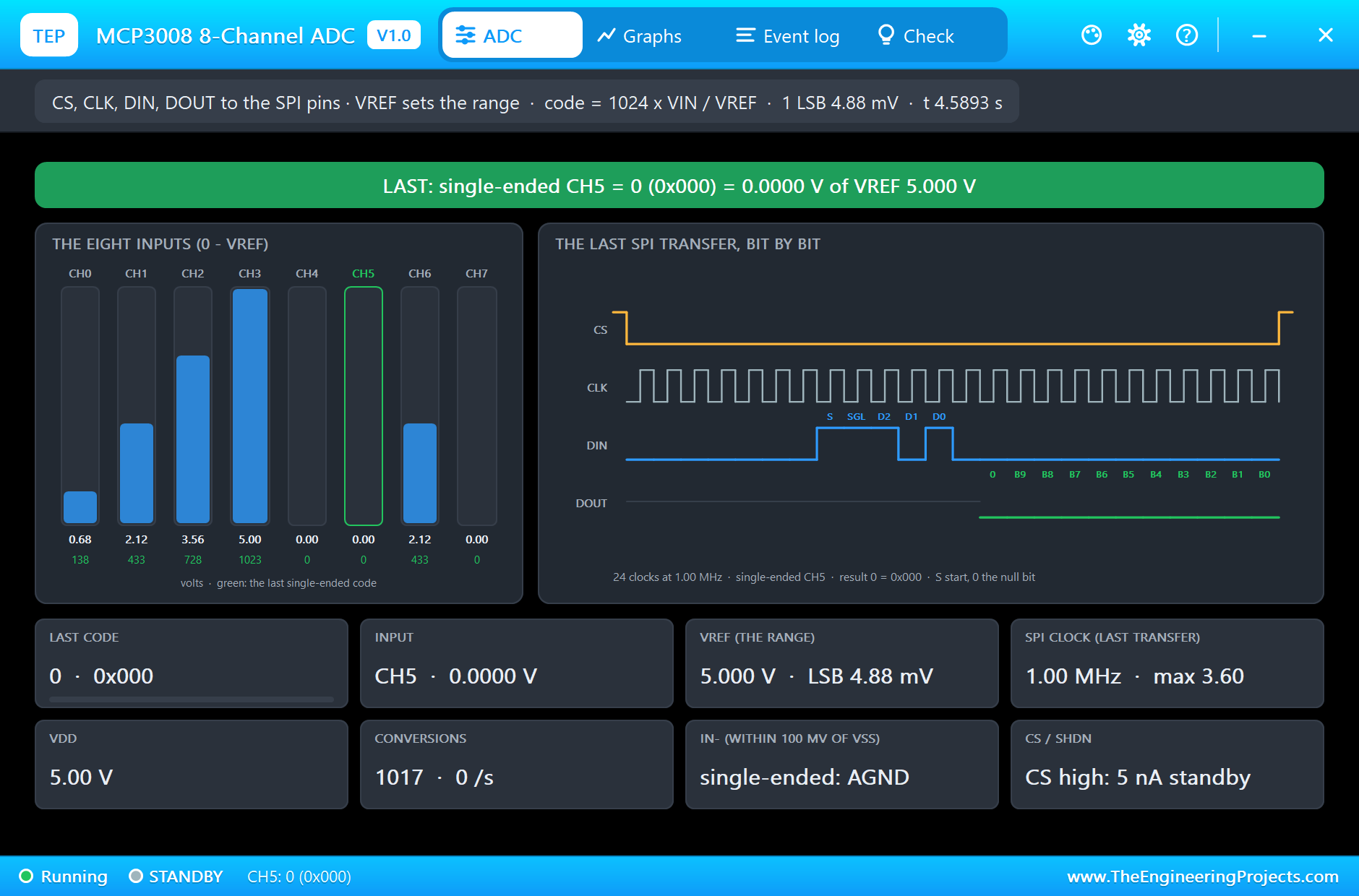
After the pause the sketch flips D4 every quarter of a second, and CH5 follows it between 0 and 1023. The input bars in the pop-up jump with it, and the timing diagram now shows D2 D1 D0 = 101 for CH5 and a result of ten ones or ten zeros.
By the end of the run the chip had made 1023 conversions.
The Graphs, the Log and the Check Page
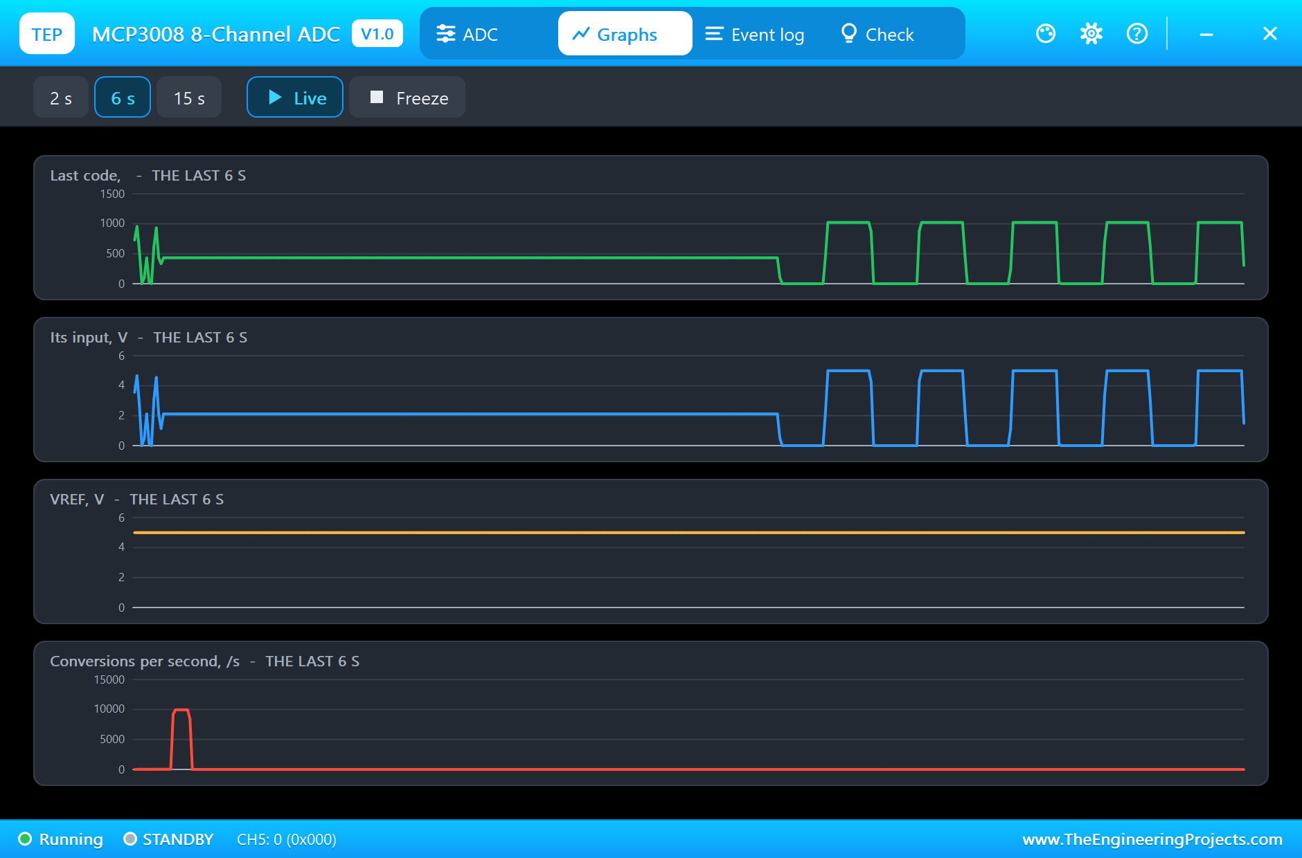
The Graphs page plots the last code, its input, VREF and the conversion rate over the last 2, 6 or 15 simulated seconds. The Event log keeps the power-on, the first conversion and the warnings: the IN- out of range and the clock over the limit.
The Check page sums up the chip: VDD and the clock it allows, VREF and the LSB, the last transfer decoded, the result worked out from the formula, the last code of every channel, the differential warnings and the conversion count.
Try It Yourself
- Connect VREF to a 2.5 V divider instead of 5 V and see the codes double and the top channels saturate at 1023.
- Read the eight channels as four differential pairs and work out each result.
- Clock 8 more bits after the result and decode the LSB-first copy.
- Raise the SPI clock step by step and watch the warning appear above 3.6 MHz; then lower VDD and see the limit fall.
- Replace the ladder with a potentiometer and plot its position.
- Average 16 readings and see how the result settles.
Ideas to Extend the Demo
- Build an eight-channel data logger that prints CSV lines for a spreadsheet.
- Read a joystick on two channels and drive a servo or an LCD cursor.
- Measure a battery through a divider and display its charge.
- Use the MCP4725 DAC from our previous library as a test signal and measure its staircase.
Your Own Sketches
The demo sketch is in the zip file, and you can change it in the Arduino IDE. New to Arduino? Start with our Arduino Tutorial for Beginners. Export the compiled binary, and set the UNO's PROGRAM property to the new file. Our guide on How to get the HEX file from Arduino shows you where the file ends up.
Things to Know Before Using a Real Chip
- Mind the clock: under 3.6 MHz at 5 V and 1.35 MHz at 2.7 V; the sample has 1.5 clocks to charge its 20 pF.
- Mind the source: high-resistance sensors charge the sample slowly; buffer them or slow the clock.
- A clean reference: a separate, quiet VREF gives cleaner results than a noisy 5 V.
- CS between conversions: CS must go high between conversions and once after power-up.
Troubleshooting
- NO SUPPLY: VDD is missing or under 2 V.
- Every result 0 or garbage: CS never went high after power-up, the SPI mode is not 0,0 or 1,1, or MISO and MOSI are swapped.
- The codes are a little off: VREF is not what the sketch assumes; measure it.
- A differential result is 0: IN+ is at or below IN-, or D0 picked the other channel as IN+.
- A clock warning: the SPI clock is over the limit for the supply; slow it down.
- The part is not simulated:
TEPMCP3008.DLLis missing from MODELS and from the project folder.
Limitations of the Simulation
- INL, DNL and the offset and gain errors (all within 1 to 1.5 LSB) are not modelled; the result is the ideal code.
- The sample capacitor charging through the source resistance is not modelled; a too-fast clock is reported, not corrupted.
- Noise on the inputs and the reference is not modelled.
- Arduino is a name of Arduino and MCP3008 of Microchip; this library is not made or endorsed by Arduino, Labcenter or Microchip.
- Tested in Proteus 8.5 in November 2026 (the demo as shipped). Proteus 7 is not supported.
So, that was all about the MCP3008 8-Channel ADC Library for Proteus. I hope it helps you build your data-acquisition project on your own PC first: eight analog inputs, the real SPI protocol drawn bit by bit, and a sketch you can move to the real chip unchanged. If you have any questions, ask in the comments and I will help you out. Till the next tutorial, take care and have fun!

Comments
0