


INA128 Instrumentation Amplifier Library for Proteus Simulation


Hello friends, I hope you all are doing great. Today, I am going to share the new INA128 Instrumentation Amplifier Library for Proteus Simulation, the fifth of the lab ICs in our University Lab series. If you have looked for a Proteus simulation of an instrumentation amplifier, this is it. Strain gauges, load cells, pressure sensors, thermocouples and ECG electrodes all give tiny signals, a few millivolts or less, sitting on top of a much larger common voltage. An ordinary op-amp circuit struggles with that. An instrumentation amplifier is built for it, and the INA128 is the one most university labs use.
INA128 Instrumentation Amplifier Library for Proteus Simulation
Latest version: V1.0 (November 2026, this tutorial)
Helping Tools
- Serial Monitor Advance: a serial terminal window for the UART of your board
- Serial Monitor Expert: the serial monitor with extra debugging tools
- LCD Library for Proteus V3.0: 16x2, 20x4 and I2C LCDs to show your readings
Our library brings the real chip into your Proteus simulation: the INA128 in its PDIP-8 package, drawn at its true size of 9.81 x 6.35 mm. The simulation model follows TI's datasheet and its three-op-amp design. The gain is set by the actual resistor you wire between pins 1 and 8, and the model measures it back from its current. It also has the internal amplifiers' limited range, the output swing, the offset, the CMRR and the bandwidth. The pop-up shows all three amplifiers inside the chip live. The demo is a Wheatstone bridge read by an Arduino: first directly, where it sees almost nothing, then through the INA128, where it resolves tens of microvolts.
NOTICE: Our team has put a lot of effort into these small parts: the bodies, the animation and the pop-ups are all our own design, and you get them free. Your feedback is the fuel that keeps us going, so please tell us what you think in the comments below or in the INA128 board of our forum. And if our free libraries help you, you can buy us a coffee. So, let's get started with the INA128 Instrumentation Amplifier Library for Proteus Simulation:
What is the INA128?
An instrumentation amplifier amplifies the difference between its two inputs and ignores what they have in common. Both inputs are high-impedance, so it does not load the sensor. Its gain is set by one resistor, and its output sits on a reference voltage of your choice. The INA128 does all that with very low offset and very high common-mode rejection, from a single 4.5 V supply up to plus and minus 18 V.
| INA128 (PDIP, VS = ±15 V, 25 °C) | |
|---|---|
| Gain | G = 1 + 50 kΩ / RG, from 1 to 10000 |
| Supply | 4.5 V to 36 V single, ±2.25 V to ±18 V; 700 uA |
| Offset (input-referred) | 10 uV + 100 uV / G typical; 50 uV + 500 uV / G maximum |
| Input bias current | 2 nA typical, 5 nA maximum |
| CMRR | 86 / 106 / 125 / 130 dB typical at G = 1 / 10 / 100 / 1000 |
| Bandwidth | 1.3 MHz / 640 kHz / 200 kHz / 20 kHz at G = 1 / 10 / 100 / 1000 |
| Slew rate | 4 V/us |
| Common-mode range | (V-) + 2 V to (V+) - 2 V with the output at 0 V |
| Output swing | 1.4 V from each supply rail |
The Pins
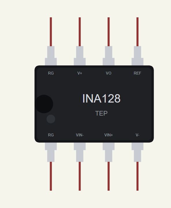
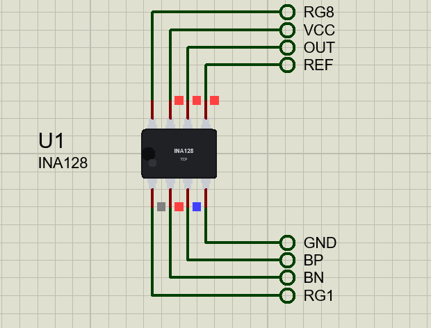
Pins 1 and 8 are RG, the gain resistor's two ends. Pin 2 is VIN-, 3 is VIN+, 4 is V-, 5 is REF, 6 is VO and 7 is V+. Our drawing lies on its side with the notch on the left: RG, VIN-, VIN+ and V- along the bottom, RG, V+, VO and REF along the top. In the netlist the two RG pins are called RG1 and RG8.
Three Op-Amps Inside
The input stage. Two amplifiers, A1 and A2, buffer the inputs. Each has a 25 kΩ resistor from its output back to its inverting input, and the two inverting inputs are the RG pins. Feedback holds pin 1 at VIN- and pin 8 at VIN+, so the voltage across RG is exactly the input difference, and the current (VIN+ - VIN-) / RG flows through RG and through both 25 kΩ resistors. The outputs of A1 and A2 move apart by (1 + 50 kΩ / RG) times the input difference. Their common voltage passes through with a gain of only 1.
The difference stage. A3 with four 40 kΩ resistors subtracts A1's output from A2's and adds REF: VO = REF + G (VIN+ - VIN-). The common voltage cancels here, and the CMRR measures how well.
The catch. A1 and A2 carry the common voltage plus half the amplified difference. They need headroom from the supply rails, about 2 V each side for the INA128. On a 5 V supply that leaves only 2 V to 3 V for them, and it is the most common surprise with this chip. The demo shows it.
Features of the INA128 Instrumentation Amplifier Library for Proteus Simulation
- The real chip at true scale: the PDIP-8, 9.81 x 6.35 mm, with its real pinout.
- The gain from your RG: wire any resistor between pins 1 and 8; the simulation model measures it and the gain follows (open gives G = 1).
- The internal limits: A1 and A2 kept 2 V from each rail, the output 1.4 V; the pop-up says which one is limiting.
- Datasheet behaviour: offset 10 uV + 100 uV / G, CMRR by gain, bandwidth by gain, 4 V/us, 2 nA bias, 700 uA supply current.
- A real REF pin: loaded by the internal 80 kΩ, so a weak REF source shows its effect as on the bench.
- A pop-up: the three amplifiers live, eight values, a 3-second scope, graphs, an event log and a check page.
- A complete package: about 1.6 MB with the library, our resistor parts, our Arduino UNO V4.0 and the demo, without the source code of the model.
The INA128 in Proteus
The device is INA128TEP in TEPINA128.LIB, under Lab ICs > Instrumentation Amps, with the prefix U and the analog model TEPINA128.DLL. Search INA128 in Pick Devices. Its one property, VOS, is the input offset in microvolts (10 by default, the datasheet's typical value); the output stage adds its own 100 uV / G. There is no gain property on purpose: the gain is whatever resistor you place between the RG pins, exactly like the real chip.
Download INA128 Instrumentation Amplifier Library for Proteus Simulation
Click the button below to download INA128-Instrumentation-Amplifier-Library-for-Proteus-v1.0.zip (about 1.6 MB, without the source code of the models):
INA128 Library for Proteus V1.0- README.txt: installation, the demo, the wiring, troubleshooting and the limits of the simulation.
- Proteus Library Files:
TEPINA128.LIB, ourTEPRESISTOR.LIBandArduinoV4TEP.LIB. - Proteus Model Files:
TEPINA128.DLL,TEPRESISTOR.DLLandTEPARDUINO.DLL. - Arduino Code: the demo sketch.
- Proteus Simulation: the demo project, its HEX file and copies of the DLLs.
No Proteus yet? Read How to Download and Install Proteus 7 and 8. New to libraries? Follow How to Install a New Library in Proteus.
How to Install INA128 Instrumentation Amplifier Library for Proteus Simulation
- Close Proteus and extract the whole zip file, for example to your Desktop.
- Copy the files from Proteus Library Files into the LIBRARY folder of Proteus.
- Copy the files from Proteus Model Files into the MODELS folder.
- Delete
TEPINA128.IDXfrom the LIBRARY folder if it is there. - Start Proteus, press P and search for INA128.
Proteus Simulation of a Wheatstone Bridge
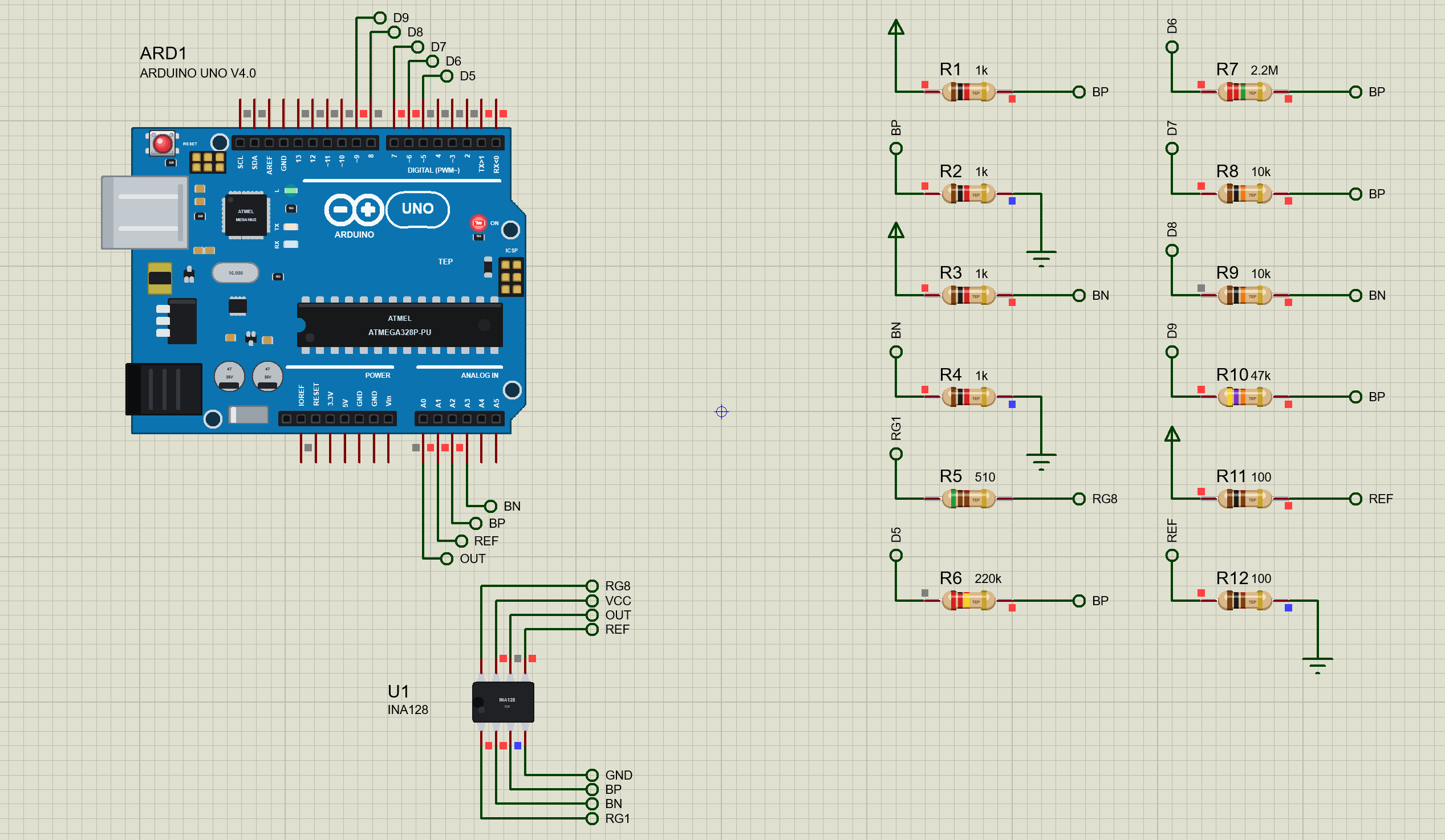
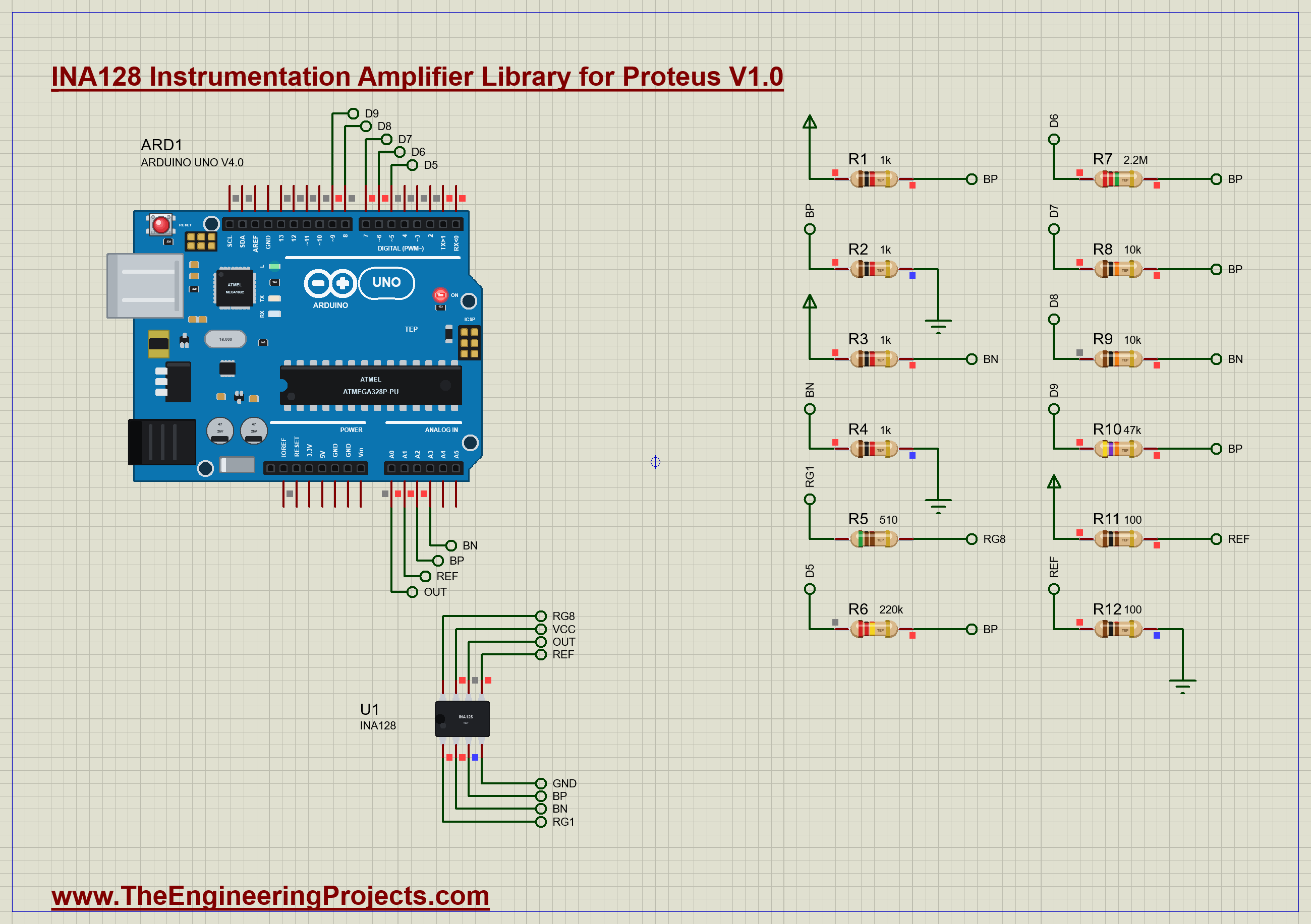
The demo has our Arduino UNO Library for Proteus V4.0 with its built-in monitor, the same window as our TEP Serial Monitor Advance for Proteus, the INA128 on the UNO's 5 V and twelve of our resistor parts. R1 to R4, 1 kΩ each, form a Wheatstone bridge, the circuit behind every strain gauge and load cell: both of its middle points, BP and BN, sit at 2.5 V. BP goes to VIN+ and BN to VIN-. R5, 510 Ω, is RG, so G = 1 + 50 / 0.51 = 99.04. REF comes from R11 and R12, two 100 Ω resistors, at 2.5 V, so the output sits in the middle of the supply when the bridge is balanced. Open INA128-Bridge-ArduinoUnoV4.pdsprj.
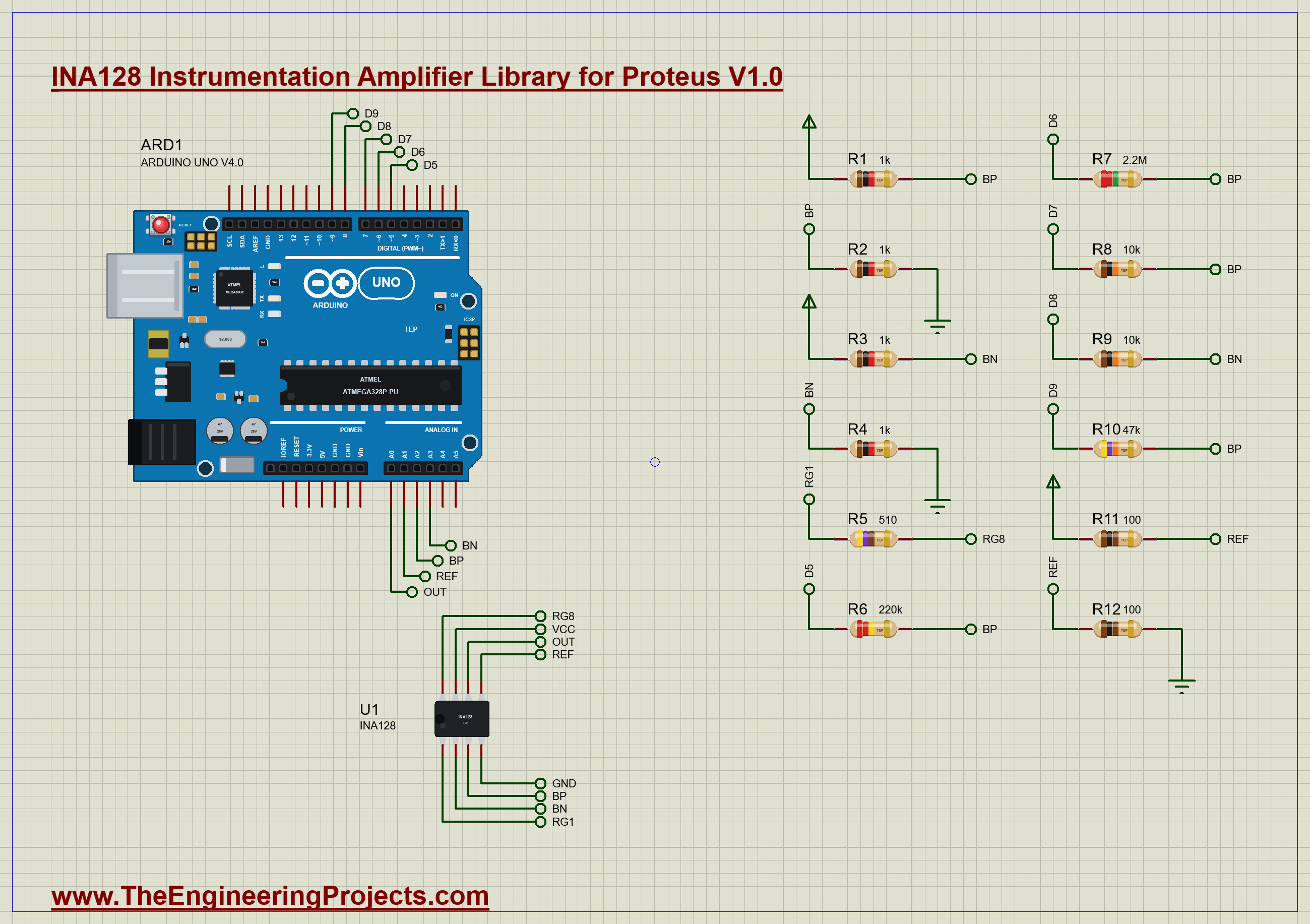
Instead of a real strain gauge, the UNO unbalances the bridge through large resistors, so the simulation is repeatable. D5 through 220 kΩ into BP shifts it by 5.67 mV; D6 through 2.2 MΩ by 0.57 mV; D7 and D8 through 10 kΩ into both sides shift both by 119 mV, a pure common-mode change; and D9 through 47 kΩ shifts BP by 26.3 mV, more than this circuit can handle. A0 reads the INA128's output, A1 reads REF, and A2 and A3 read the bridge directly, for comparison.
The Sketch
Each control pin has three states: HIGH pushes current into the bridge, LOW pulls it out, and INPUT, high impedance, leaves the bridge alone:
void drive(int pin, int level) {                                              // 1 HIGH, -1 LOW, 0 high impedance
  if (level == 0) pinMode(pin, INPUT);
  else if (level > 0) { digitalWrite(pin, HIGH); pinMode(pin, OUTPUT); }
  else { pinMode(pin, OUTPUT); digitalWrite(pin, LOW); }
}
For each state it prints two numbers: the bridge as the UNO sees it alone (A2 - A3) and the INA128's output relative to REF (A0 - A1), each the average of 16 readings, in millivolts:
float out = 1000 * (readV(A0) - readV(A1)), bridge = 1000 * (readV(A2) - readV(A3));Dividing the output by the gain gives the input difference the INA128 saw:
const float G = 1 + 50000.0 / 510;After the eight states, D5 keeps switching HIGH, off, LOW, off every 300 ms, for the pop-up's scope.
INA128 Simulation Results
Open the project and press Run. The demo runs about 13 simulated seconds, which Proteus ran in under three minutes on our PC with the pop-up open. Click the chip to open its pop-up; every number below comes from one simulation run, the demo exactly as it ships.
The Gain From RG
The first line of the Event log is the gain. The simulation model measures the current through the resistor on pins 1 and 8 and works back to RG: 510.00 Ω, so G = 99.0393, the 99.04 the formula promises. Change R5 and the gain follows; remove it and the gain drops to 1.
Microvolts the UNO Cannot See
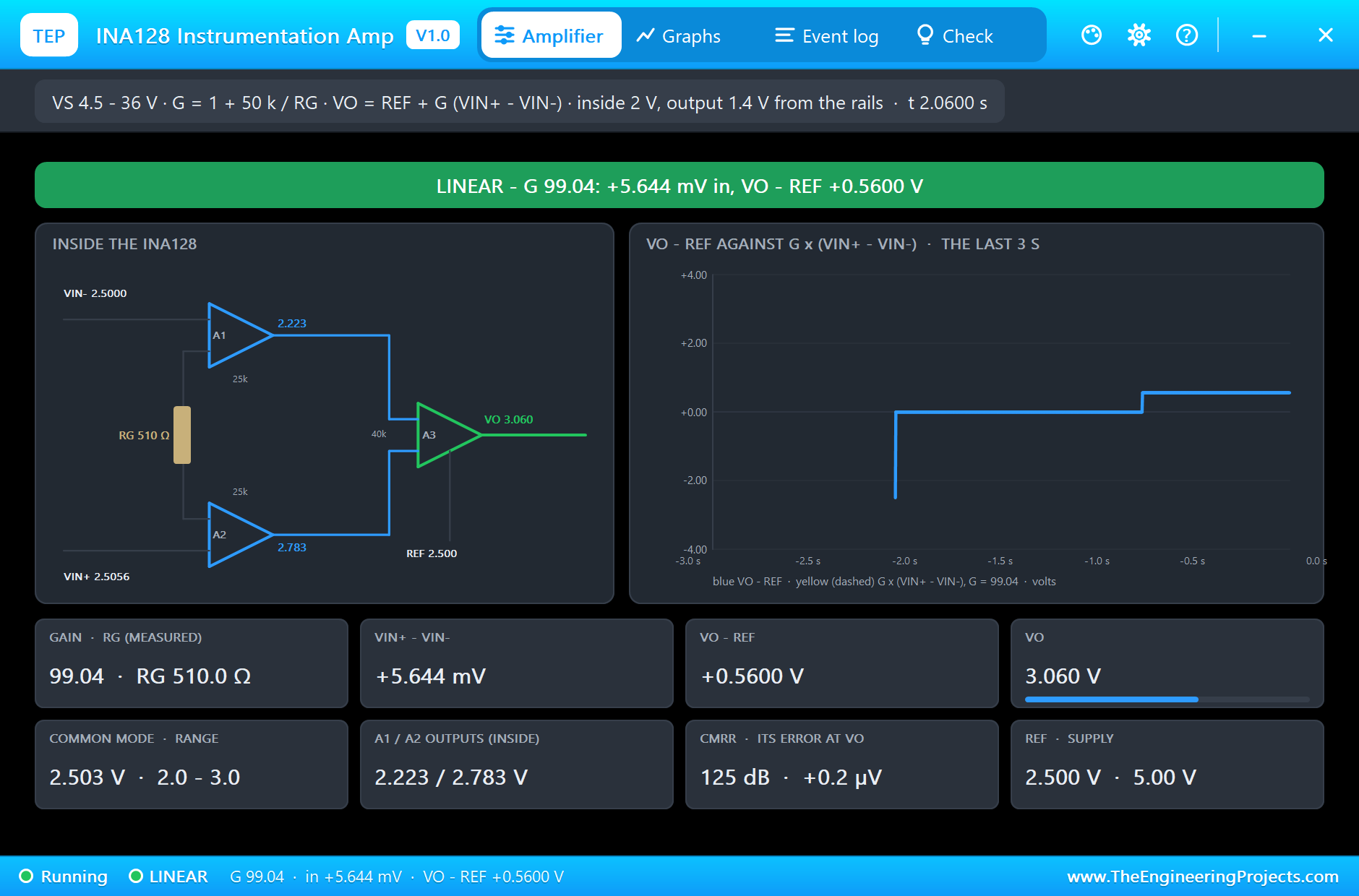
With D5 HIGH, the bridge is unbalanced by 5.644 mV in the simulation (the resistor sum gives 5.67 mV; the UNO's pins load BP very slightly). Read directly, that is about one step of the UNO's converter (4.9 mV): the monitor shows the bridge as 4.9 mV, the nearest value the UNO can show. Through the INA128 the output moves 0.5600 V, and the UNO reads 562.1 mV, which is 5.675 mV at the input. One step of the UNO now means 49 uV at the bridge.
Inside the chip, the pop-up shows A1 at 2.2228 V and A2 at 2.7828 V: they moved apart by G times the input, and their average is still the bridge's 2.5 V. A3 subtracts them and adds REF: VO 3.0602 V, REF 2.5002 V. With D5 LOW everything mirrors, and the UNO reads -562.1 mV.
With D6 HIGH, the bridge moves only 0.57 mV. The UNO alone sees nothing at all; through the INA128 it reads 53.8 mV, 0.543 mV at the input, within one of its steps of the true value.
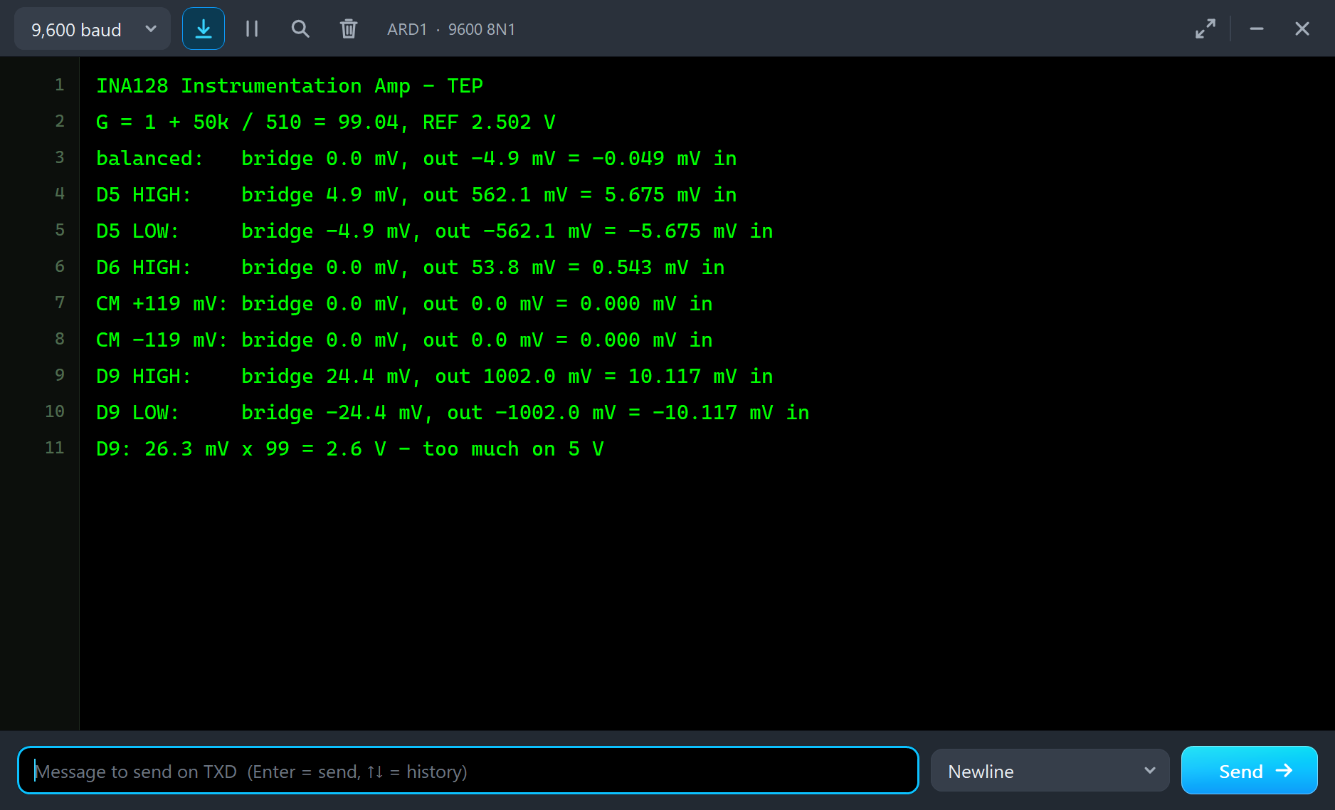
A note on the "balanced" line: the UNO reads -4.9 mV there. That is one step of its converter, not the INA128. The INA128's real output offset is 10 uV x 99 + 100 uV = 1.09 mV, smaller than one UNO step, and whether VO and REF round to the same step or to neighbouring steps decides between 0 and -4.9 mV.
Common Mode: 119 mV That Do Not Matter
Now D7 and D8 push both sides of the bridge up together. In the simulation both inputs rise to 2.6188 V, 119 mV higher, and the UNO reads exactly 0.0 mV from the INA128, as it does when D7 and D8 pull both sides down. That is common-mode rejection. The pop-up shows A1 and A2 both at 2.619 V: they simply followed. The CMRR tile gives the size of what is left: at G = 99 the INA128's CMRR is 125 dB, so 119 mV of common mode moves the output by 6.7 uV, a million times below the signal.
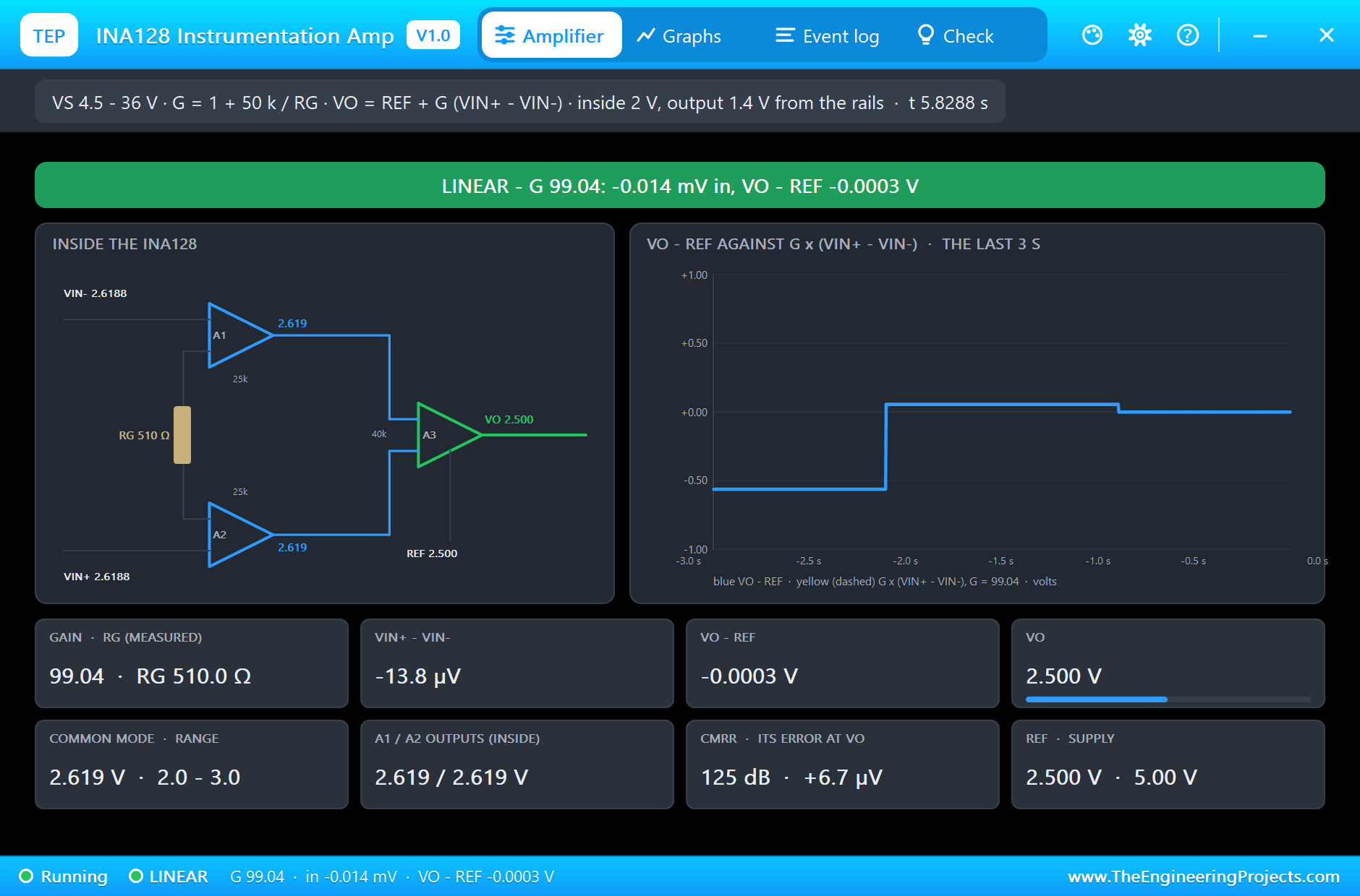
This is why the REF pin needs a low-impedance source. Inside the chip REF is loaded by 80 kΩ, and our 100 Ω divider is a 50 Ω source, so REF itself moves by 50 / 80 000 of whatever A2 does. Here that is 74 uV for the 119 mV common-mode step, harmless, but a 10 kΩ divider would be 100 times worse. TI recommends a voltage reference or an op-amp buffer on REF.
Too Much for 5 V: the Input Stage Limit
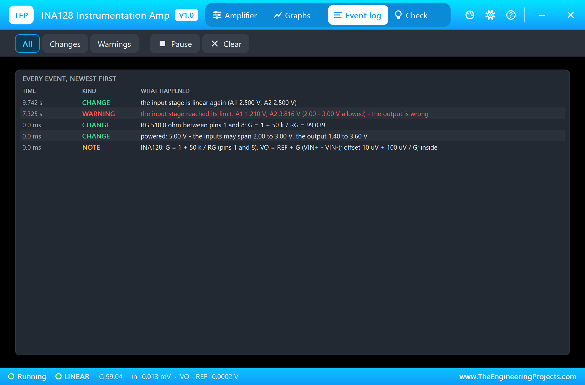
D9 HIGH unbalances the bridge by 26.304 mV. Times 99 that asks for 2.6 V on top of REF, and the output could swing up to 3.6 V on a 5 V supply. But the output stops at 3.5004 V, VO - REF = +1.0001 V, and the UNO reads 1002.0 mV. The output stage is not the problem. The pop-up's banner turns orange and names it: A2 would need 3.816 V and A1 1.210 V, but on 5 V they can only work between 2.00 and 3.00 V. Each stops 0.5 V from 2.5 V, and A3 can only report the 1.0 V between them. The Event log records the limit once it has lasted 50 us, and "linear again" when D9 is released.
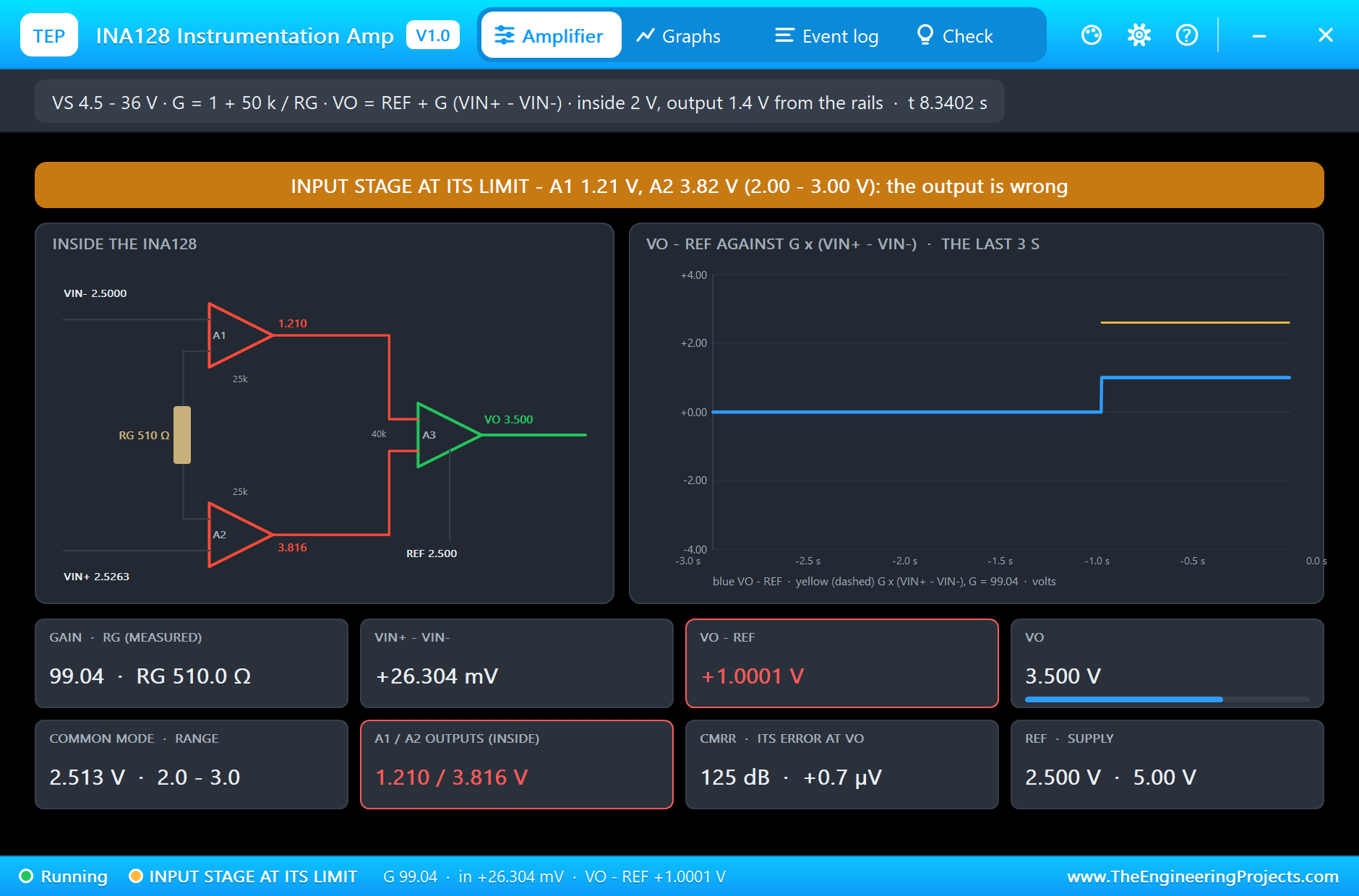
Meanwhile the UNO alone reads the bridge as 24.4 mV, five of its steps: the signal is big enough to see directly now, and too big for the INA128 at this gain on this supply. On 5 V, at G = 99, this INA128 circuit handles about plus or minus 10 mV. A lower gain, a bigger supply or a rail-to-rail instrumentation amplifier extends that.
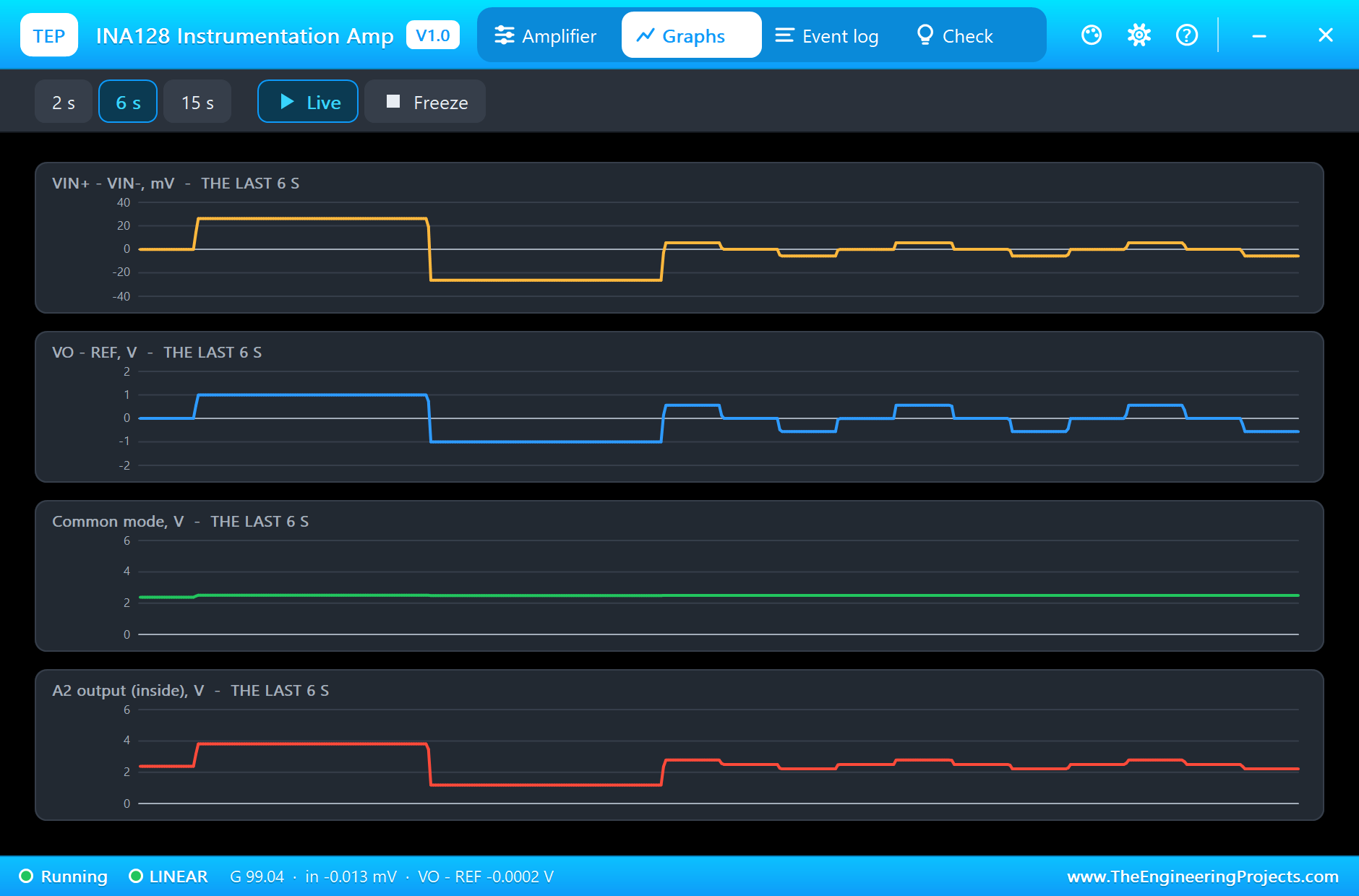
The Graphs, the Log and the Check Page
The Graphs page plots the input difference, VO - REF, the common mode and A2's output over the last 2, 6 or 15 simulated seconds: the D5 steps, the common-mode bump that leaves VO - REF flat, and the D9 step where A2 hits its 3 V ceiling. The Event log lists the gain found at the start, the input-stage limit and its end.
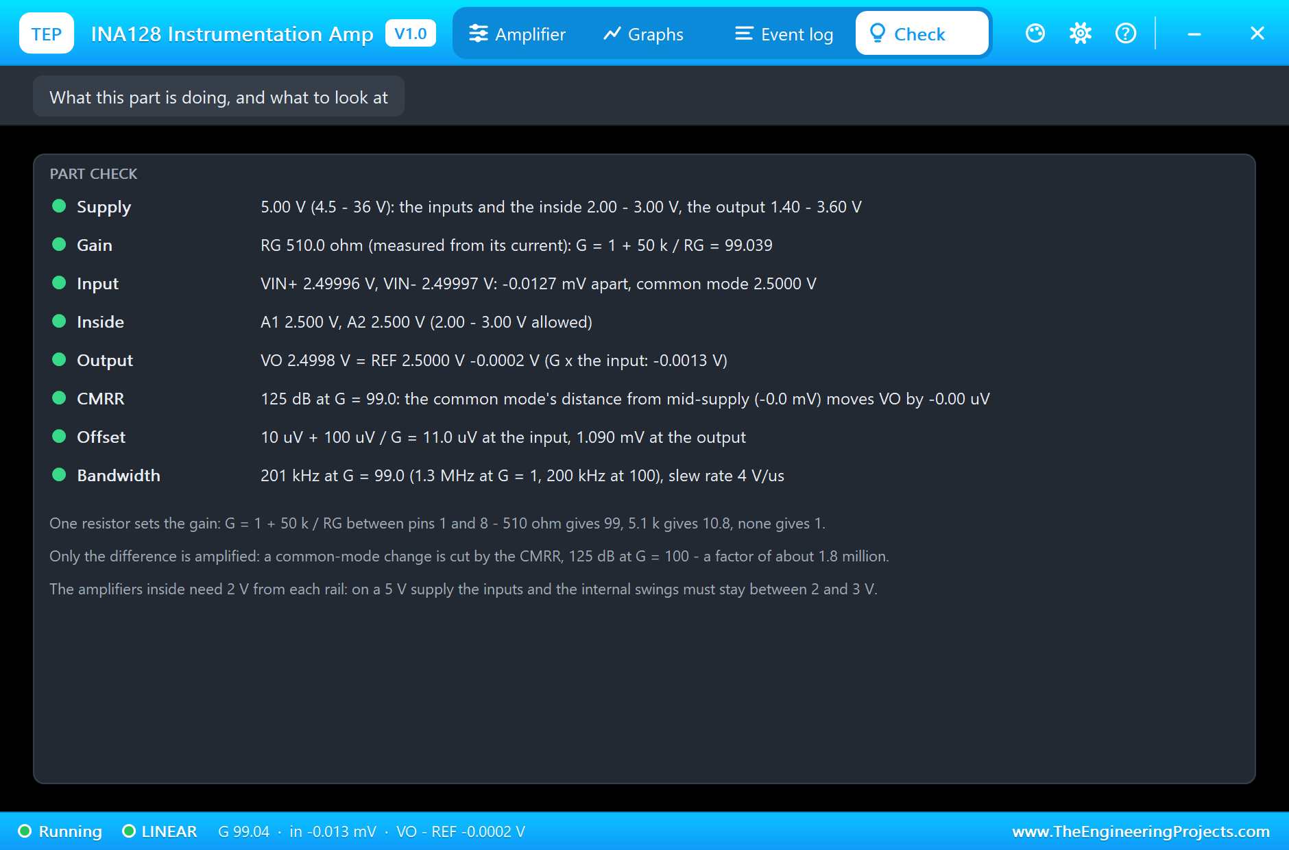
The Check page sums up the chip: the supply and the ranges it allows, RG and the gain, the inputs, the inside, the output against G times the input, the CMRR at this gain with its error, the offset at the input and the output, and the bandwidth.
Try It Yourself
- Change R5 to 5.1 kΩ for G = 10.8 and drive D9: the output follows the 26 mV all the way now.
- Remove R5 and see G = 1: the INA128 becomes a precise difference amplifier.
- Set VOS to 50 (the maximum) and watch the balanced output move by about 5 mV.
- Run the INA128 from +12 V and see the internal range widen to 2 V to 10 V.
- Replace R11 and R12 with 10 kΩ and compare REF and VO during the common-mode test.
- Unbalance the bridge by changing R2 to 1.02 kΩ, a 2 % change of one arm, and read it through the INA128.
Ideas to Extend the Demo
- Build a kitchen scale: a load cell is a Wheatstone bridge, and the INA128 reads it the same way.
- Add an RC filter on VO and average in the sketch for slow sensors.
- Read a thermocouple: a few tens of microvolts per degree, perfect for a gain of 500 or more.
- Read VO with the MCP3008 ADC from our earlier library, its VREF on a stable reference.
Your Own Sketches
The demo sketch is in the zip file, and you can change it in the Arduino IDE. New to Arduino? Start with our Arduino Tutorial for Beginners. Export the compiled binary, and set the UNO's PROGRAM property to the new file. Our guide on How to get the HEX file from Arduino shows you where the file ends up.
Things to Know Before Using a Real Chip
- Mind the internal range on 5 V: A1 and A2 need 2 V from each rail; at high gain the usable input is only millivolts. A rail-to-rail part (INA333, INA826) suits 5 V better.
- Drive REF from a low impedance: a reference or an op-amp buffer; a plain divider costs CMRR and gain accuracy.
- RG sets everything: use a 1 % or better resistor with a low temperature coefficient, close to pins 1 and 8.
- Give the inputs a bias path: floating sources such as thermocouples need resistors to a mid voltage.
Troubleshooting
- NO SUPPLY: V+ - V- is under 4 V; a warning appears below 4.5 V.
- G = 1: nothing between pins 1 and 8; fit RG.
- INPUT STAGE AT ITS LIMIT: an internal amplifier needs more than the supply allows; lower the gain or bring the inputs to mid-supply.
- OUTPUT AT ITS LIMIT: VO is within 1.4 V of a rail; move REF or lower the gain.
- The output is offset: check REF; a weak divider sags.
- The part is not simulated:
TEPINA128.DLLis missing from MODELS and from the project folder.
Limitations of the Simulation
- The common-mode range is a rectangle in the simulation (2 V from each rail inside, 1.4 V at the output); the real chip's range is a hexagon that depends on the output voltage.
- Noise, drift and the power-supply rejection are not modelled.
- The output current limit is not modelled; currents over 15 mA are reported on the Check page.
- Arduino is a name of Arduino and INA128 is a part number of Texas Instruments; this library is not made or endorsed by Arduino, Labcenter or Texas Instruments.
- Tested in Proteus 8.5 in November 2026 (the demo as shipped). Proteus 7 is not supported.
So, that was all about the INA128 Instrumentation Amplifier Library for Proteus Simulation. I hope it helps you design your sensor front ends in a simulation first: real gain from a real resistor, real common-mode rejection, and the internal limits that catch everyone on a 5 V supply. If you have any questions, ask in the comments and I will help you out. Till the next tutorial, take care and have fun!

Comments
0